Support plate hole filling process based on metal imprinting

A carrier plate and metal technology, which is applied in the field of hole filling process of carrier plate based on metal imprinting, can solve problems such as low efficiency, stress concentration, affecting filling efficiency, etc., and achieve simple and convenient process steps, matching thermal expansion coefficient, and improving filling efficiency. Effect

Pending Publication Date: 2021-10-22
GUANGDONG UNIV OF TECH
View PDF4 Cites 0 Cited by
  • Summary
  • Abstract
  • Description
  • Claims
  • Application Information

AI Technical Summary

Problems solved by technology

At present, the realization of through hole and blind hole interconnection structure mainly adopts electroplating copper hole filling technology; however, using electroplating solution to fill holes has the following disadvantages: (1) In the process of microhole filling, it is easy to produce Holes, gap filling and other defects; on the one hand, it affects the electrical and thermal conductivity of through holes and blind holes; on the other hand, due to the mismatch of thermal expansion coefficients between copper and substrate materials, it is easy to cause stress concentration, induce cracks and lead to failure
(2) In order to avoid filling defects, the electroplating copper hole filling process needs to use lower current, which affects the filling efficiency; for large-sized holes (>10μm), the electroplating copper hole filling efficiency is extremely low

Method used


Image

  • Support plate hole filling process based on metal imprinting
  • Support plate hole filling process based on metal imprinting
  • Support plate hole filling process based on metal imprinting

Examples


Embodiment 1

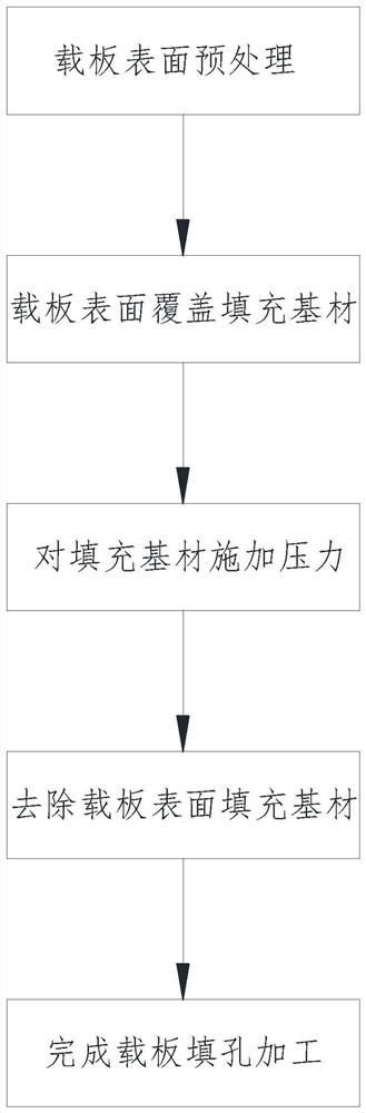
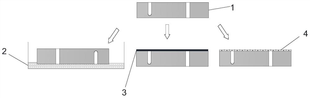
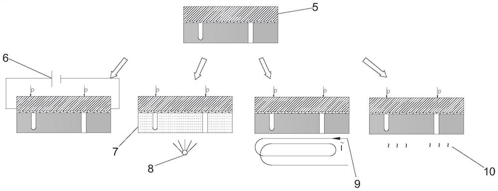
[0036] see Figure 1-Figure 4 , the carrier board hole filling process based on metal imprinting in this embodiment is characterized in that it includes the following steps:

[0037] (1) Pretreatment is performed on the surface of the substrate 1 to be filled, so that the surface of the substrate 1 and the metal do not have bonding force.

[0038] (2) Covering the filling base material 5 made of metal evenly on the surface of the carrier plate 1 .

[0039] (3) Under a controllable atmosphere, apply a downward pressure perpendicular to the surface of the carrier plate 1 on the filling substrate 5, the pressure range is 0-500Mpa; at the same time, localized heating is performed on the filling substrate 5, and the heating temperature control range is at room temperature -2000°C, so that the filling substrate 5 is deformed and pressed into the through hole or blind hole on the carrier plate 1 .

[0040] (4) Separating the carrier board 1 and the filling substrate 5 covering the s...

Embodiment 2

[0057] This embodiment discloses a specific example of hole filling on a carrier: the carrier is a ceramic carrier, and the ceramic carrier is provided with through holes with a diameter of 30 μm and a depth of 100 μm. specifically:

[0058] (1) Depositing a layer of graphite with a thickness of 10 nm on the surface of the ceramic carrier, so that the surface treatment layer of the ceramic carrier has no binding force with the metal.

[0059] (2) A copper block (filling base material) with a flat surface and a thickness of 20 nm is covered on the ceramic carrier.

[0060] (3) In a nitrogen environment, apply a pressure of 200MPa perpendicular to the ceramic carrier to the copper block, and at the same time apply a 20MHz alternating electric field to one side of the ceramic carrier to heat the surface of the copper block near the ceramic carrier, As a result, the copper block is deformed and pressed into the via, completing the filling.

[0061] (4) The copper block on the su...

Embodiment 3

[0064] This embodiment discloses another specific example of hole filling on a carrier: the carrier is a ceramic carrier, and the ceramic carrier is provided with through holes with a diameter of 15 μm and a depth of 50 μm. specifically:

[0065] (1) Deposit a layer of graphite with a thickness of 30nm on the surface of the ceramic carrier, so that the surface treatment layer of the ceramic carrier has no binding force with the metal.

[0066] (2) A copper block (filling base material) with a flat surface and a thickness of 100 nm is covered on the ceramic carrier.

[0067] (3) In a nitrogen environment, apply a pressure of 100 MPa perpendicular to the carrier plate to the copper block, and control the ambient temperature to 150°C, so that the overall temperature of the copper block will be deformed and pressed into the through hole to complete the filling.

[0068] (4) Grinding off the copper block on the surface of the ceramic carrier plate by means of mechanical grinding, ...


PUM


Abstract

The invention discloses a support plate porefilling process based on metal imprinting, which comprises the following steps of: (1) pretreating the surface of a support plate to be porefilled, so that the surface of the support plate and metal have no binding force; (2) covering the filling base material on the surface of the carrier plate; (3) applying downward pressure perpendicular to the surface of the carrier plate to the filling base material, so that the filling base material deforms and is pressed into the through hole or the blind hole in the carrier plate; (4) carrying out separation treatment on the carrier plate and the filling base material covering the surface of the carrier plate, removing the filling base material on the surface of the carrier plate, and enabling the metal in the through hole or the blind hole in the carrier plate to be still kept inside, thereby completing the hole filling processing of the carrier plate. According to the invention, rapid hole filling of the carrier plate is realized, so that an interconnection structure of through holes and blind holes is realized. The method is good in filling effect, and conductive and heat-conducting properties of the through hole and the blind hole can be improved.

Description

technical field [0001] The invention relates to a circuit carrier board filling technology, in particular to a carrier board hole filling process based on metal stamping. Background technique [0002] As one of the core technologies of semiconductor and integrated circuit manufacturing, carrier board hole filling technology can obtain through-hole and blind-hole interconnection structures, which has the advantages of reducing time delay, reducing energy consumption, and improving integration. At present, the realization of through hole and blind hole interconnection structure mainly adopts electroplating copper hole filling technology; however, using electroplating solution to fill holes has the following disadvantages: (1) In the process of microhole filling, it is easy to produce Holes, gap filling and other defects; on the one hand, it affects the electrical and thermal conductivity of through holes and blind holes; on the other hand, due to the mismatch of thermal expans...

Claims


Application Information

Patent Timeline
Patent Type & Authority Applications(China)
IPC IPC(8): H05K3/40H05K3/42
CPCH05K3/40H05K3/42
Inventor 杨冠南姚可夫黄钰森崔成强
Owner GUANGDONG UNIV OF TECH
Why Eureka
Try Eureka