Image sensor and forming method thereof

An image sensor and graphic technology, applied in radiation control devices, etc., can solve problems such as abnormal imaging of imaging pixel units and deformation of microlens shapes, and achieve the effects of avoiding damage, improving imaging quality, and realizing PDAF and imaging functions

Pending Publication Date: 2022-07-08
UNITED MICROELECTRONICS CENT CO LTD
View PDF0 Cites 0 Cited by
  • Summary
  • Abstract
  • Description
  • Claims
  • Application Information

AI Technical Summary

Problems solved by technology

[0006] However, the process of forming different curvatures usually affects the microlens of the imaging pixel unit, resulting in deformation of the microlens shape of the imaging pixel unit around the PDAF pixel unit, and in severe cases, abnormal imaging of the imaging pixel unit

Method used


Image

  • Image sensor and forming method thereof
  • Image sensor and forming method thereof
  • Image sensor and forming method thereof

Examples


Embodiment Construction

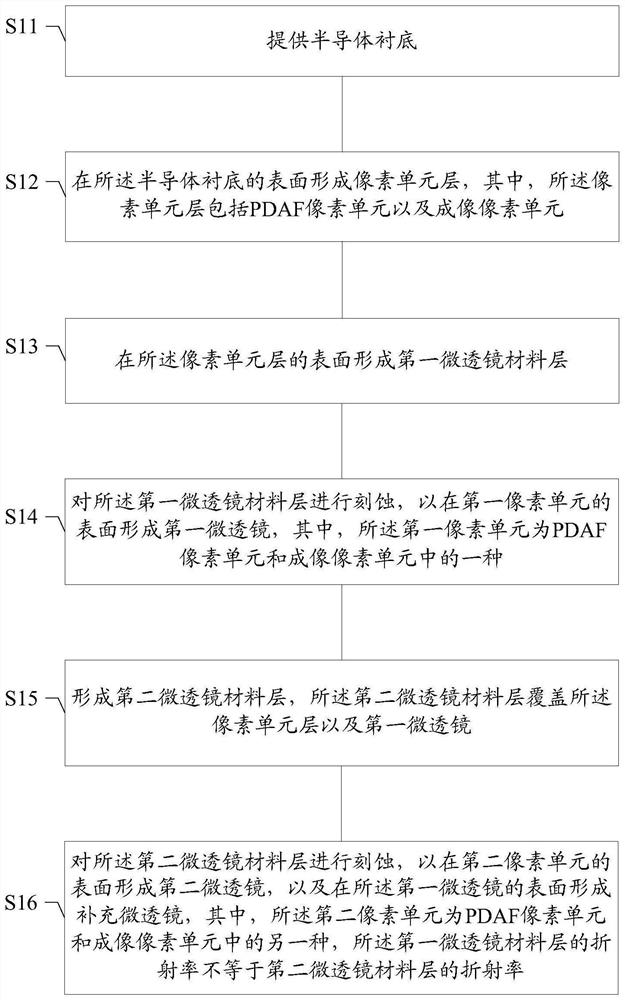
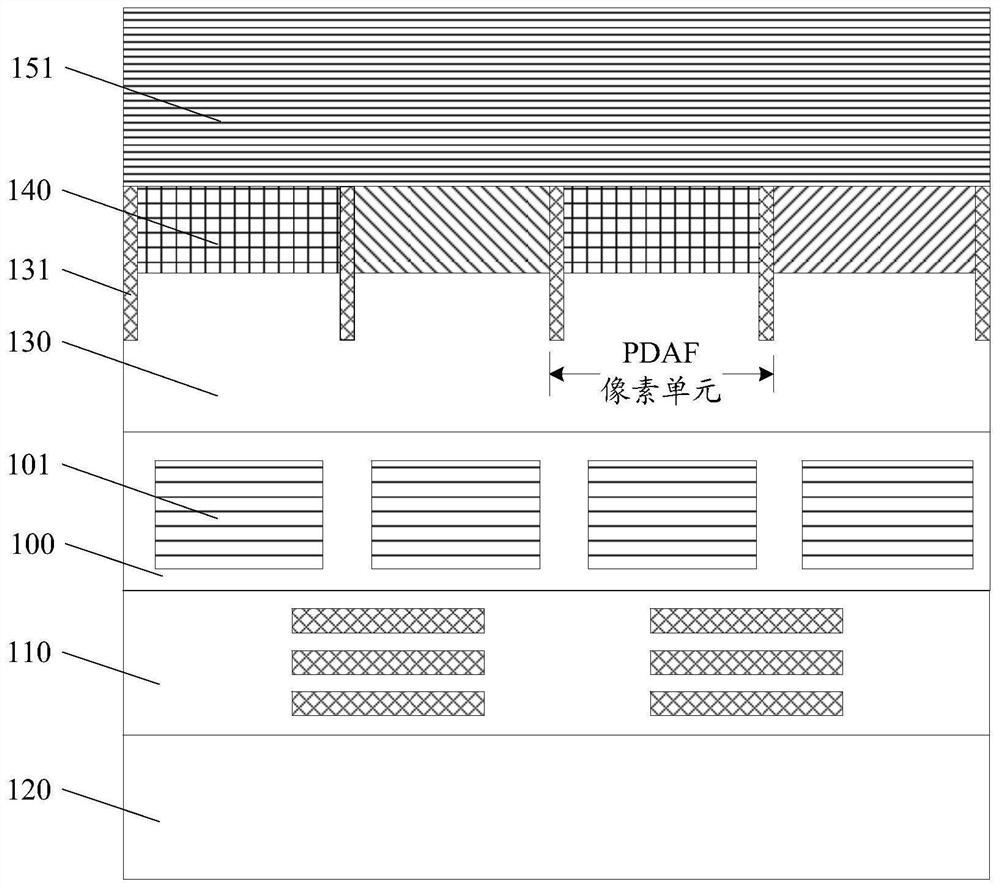
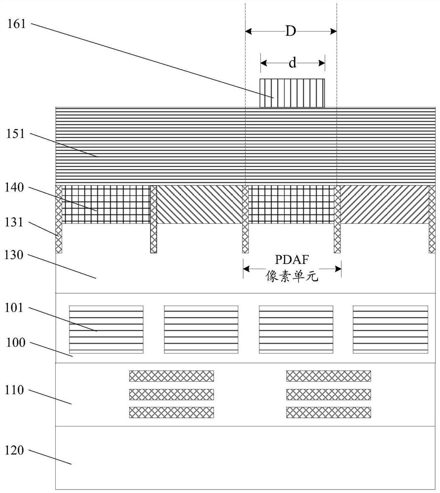
[0027] As mentioned above, in the prior art, in order to improve the performance of the optical image sensor, the PDAF technology is used for focusing. Lenses, different microlens curvatures can be used. For example, the surface of the microlens on which the PDAF pixel unit is arranged has a higher degree of curvature and a larger curvature.

[0028] The inventor of the present invention has found through research that in the prior art, the PDAF function and the imaging function are realized by using different microlens curvatures, and the processes of forming different curvatures usually have an impact on the microlenses of the imaging pixel unit, resulting in PDAF pixels. The shape of the microlens of the imaging pixel unit around the unit is deformed. For example, when the surface curvature of the microlens of the PDAF pixel unit is higher, the surface curvature of the microlens of the imaging pixel unit around the PDAF pixel unit is also higher than normal. The degree of ...


PUM


Abstract

The invention discloses an image sensor and a forming method thereof. The method comprises the steps of providing a semiconductor substrate; forming a pixel unit layer, wherein the pixel unit layer is located on the surface of the semiconductor substrate; forming a first micro lens material layer on the surface of the pixel unit layer; etching the first micro lens material layer to form a first micro lens on the surface of the first pixel unit; forming a second micro lens material layer, wherein the second micro lens material layer covers the pixel unit layer and the first micro lens; etching the second micro-lens material layer to form a second micro-lens on the surface of the second pixel unit and form a supplementary micro-lens on the surface of the first micro-lens; wherein the refractive index of the first micro-lens material layer is not equal to that of the second micro-lens material layer. According to the invention, the PDAF function and the imaging function can be realized respectively, and the influence on the imaging quality of the imaging pixel unit is effectively avoided.

Description

technical field [0001] The present invention relates to the technical field of semiconductor manufacturing, and in particular, to an image sensor and a method for forming the same. Background technique [0002] The image sensor is the core component of the camera equipment, and realizes the image capturing function by converting the optical signal into the electrical signal. Taking complementary metal-oxide-semiconductor image sensors (CMOS Image Sensors, CIS) as an example, it has been widely used in various fields due to its advantages of low power consumption and high signal-to-noise ratio. [0003] In the prior art, in order to improve the performance of the optical image sensor, the phase detection auto focus (PDAF) technology is used for focusing. The PDAF technology is based on the principle of phase difference to focus, which helps to improve the focusing speed and improve the focusing effect. , to determine the correct position of the lens so that the image is not ...

Claims


Application Information

Patent Timeline
IPC IPC(8): H01L27/146
CPCH01L27/14627H01L27/14603H01L27/14643H01L27/14685
Inventor 张舒黄晓橹陈世杰张斌
Owner UNITED MICROELECTRONICS CENT CO LTD
Why Eureka
Try Eureka