Bipolar photodiode based on gallium nitride heterojunction thin film and preparation method thereof
A photodiode and heterojunction technology, which is applied in the manufacture of circuits, electrical components, and final products, can solve problems such as integration and mass production that are difficult to achieve, and achieve the effects of excellent chemistry, good device reliability, and small size
- Summary
- Abstract
- Description
- Claims
- Application Information
AI Technical Summary
Problems solved by technology
Method used
Image

Examples
Embodiment 1
[0041] The specific implementation steps are as follows:
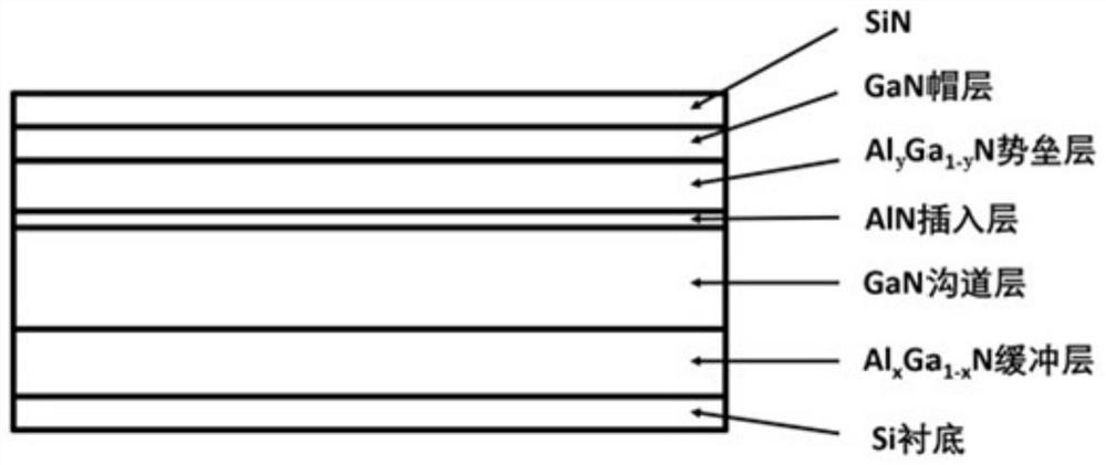
[0042] (1) A GaN heterojunction epitaxial wafer was grown by MOCVD on a 6-inch Si (111) substrate. The structure includes: 200 nm undoped AlN layer, 300 nm undoped Al 0.8 Ga 0.2 N layer, 500 nm undoped Al 0.6 Ga 0.4 N layer, 500 nm undoped Al 0.4 Ga 0.6 N layer, 300 nm undoped Al 0.2 Ga 0.8 N layer, 2 μm undoped GaN layer, 1 nm undoped AlN layer, 20 nm undoped Al 0.25 Ga 0.75 N layer, 3nm undoped GaN layer, 5 nm SiN layer, such as figure 1 shown;
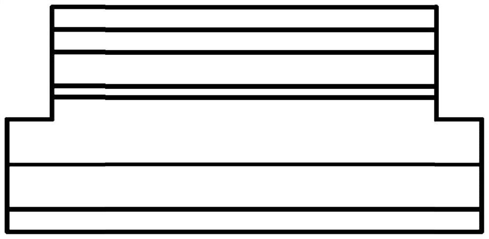
[0043] (2) On the wafer surface described in step (1), the working area of the device is defined by ultraviolet lithography. The working area of this embodiment is 100×230 μm 2 . Then pass chlorine (Cl 2 ) Inductively Coupled Plasma (ICP) dry etching of areas outside the working area, Cl 2 The flow rate is 15 sccm, the power is 150W, and the etching depth is 150 nm to realize the isolation of a single device, such as figure 2 shown;
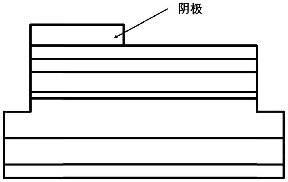
[0044] (3) The wafer...
Embodiment 2
[0052] The specific implementation steps are as follows:
[0053] (1) GaN heterojunction epitaxial wafers were grown by MOCVD on a 6-inch Si (111) substrate. The structure includes: 150 nm undoped AlN layer, 250 nm undoped Al 0.8 Ga 0.2 N layer, 300 nm undoped Al 0.6 Ga 0.4 N layer, 500 nm undoped Al 0.4 Ga 0.6 N layer, 400 nm undoped Al 0.2 Ga 0.8 N layer, 1.5 μm undoped GaN layer, 0.5 nm undoped AlN layer, 30 nm undoped Al 0.25 Ga 0.75 N layer, 4 nm undoped GaN layer, 4 nm SiN layer;
[0054] (2) On the wafer surface described in step (1), the working area of the device is defined by ultraviolet lithography. The working area of this embodiment is 100×230 μm 2 . Then pass chlorine (Cl 2 ) Inductively Coupled Plasma (ICP) dry etching of areas outside the working area, Cl 2 The flow rate is 15 sccm, the power is 150W, and the etching depth is 200 nm to realize the isolation of a single device;
[0055] (3) The wafer obtained in step (2) is degummed and cleaned....
Embodiment 3
[0063] The specific implementation steps are as follows:
[0064] (1) A GaN heterojunction epitaxial wafer was grown by MOCVD on a 6-inch Si (111) substrate. The structure includes: 100 nm undoped AlN layer, 200 nm undoped Al 0.8 Ga 0.2 N layer, 400 nm undoped Al 0.6 Ga 0.4 N layer, 400 nm undoped Al 0.4 Ga 0.6 N layer, 500 nm undoped Al 0.2 Ga 0.8 N layer, 1.2 μm undoped GaN layer, 0.7 nm undoped AlN layer, 15 nm undoped Al 0.25 Ga 0.75 N layer, 5 nm undoped GaN layer, 3 nm SiN layer;
[0065] (2) On the wafer surface described in step (1), the working area of the device is defined by ultraviolet lithography. The working area of this embodiment is 100×230 μm 2 . Then pass chlorine (Cl 2 ) Inductively Coupled Plasma (ICP) dry etching of areas outside the working area, Cl 2The flow rate is 15 sccm, the power is 150W, and the etching depth is 150 nm to realize the isolation of a single device;
[0066] (3) The wafer obtained in step (2) is degummed and cleaned. ...
PUM
| Property | Measurement | Unit |
|---|---|---|
| thickness | aaaaa | aaaaa |
| thickness | aaaaa | aaaaa |
| thickness | aaaaa | aaaaa |
Abstract
Description
Claims
Application Information
 - R&D Engineer
- R&D Manager
- IP Professional
- Industry Leading Data Capabilities
- Powerful AI technology
- Patent DNA Extraction
Browse by: Latest US Patents, China's latest patents, Technical Efficacy Thesaurus, Application Domain, Technology Topic.
© 2024 PatSnap. All rights reserved.Legal|Privacy policy|Modern Slavery Act Transparency Statement|Sitemap