Light-emitting diode chip capable of improving cracks of insulating layer and preparation method of light-emitting diode chip

A technology of light emitting diodes and insulating layers, applied in semiconductor devices, electrical components, circuits, etc., can solve problems such as easy cracks, and achieve the effect of improving quality

Pending Publication Date: 2022-07-12
HC SEMITEK ZHEJIANG CO LTD
View PDF0 Cites 2 Cited by
  • Summary
  • Abstract
  • Description
  • Claims
  • Application Information

AI Technical Summary

Problems solved by technology

[0005] Embodiments of the present disclosure provide a light-emitting diode chip that improves cracks in the insulating layer and its preparation method, which can improve the problem that cracks easily occur when the insulating layer extends to the semiconductor layer at the vertical corner of the electrode, and improve the quality of the light-emitting diode chip

Method used


Image

  • Light-emitting diode chip capable of improving cracks of insulating layer and preparation method of light-emitting diode chip
  • Light-emitting diode chip capable of improving cracks of insulating layer and preparation method of light-emitting diode chip
  • Light-emitting diode chip capable of improving cracks of insulating layer and preparation method of light-emitting diode chip

Examples


Embodiment Construction

[0037] In order to make the objectives, technical solutions and advantages of the present disclosure clearer, the embodiments of the present disclosure will be further described in detail below with reference to the accompanying drawings.

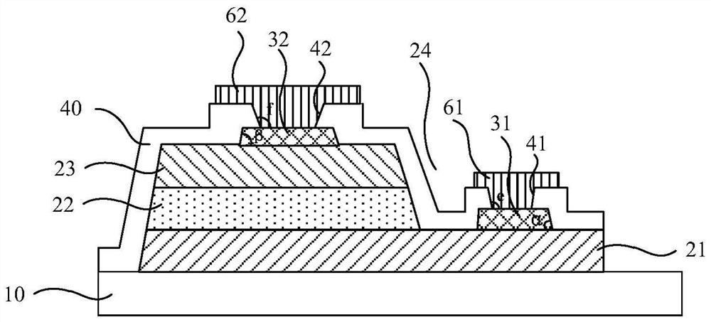
[0038] figure 1 It is a schematic structural diagram of a light emitting diode chip provided by an embodiment of the present disclosure. like figure 1 As shown, the light emitting diode chip for improving cracks in the insulating layer includes: a substrate 10 , an epitaxial layer 20 , a first electrode 31 , a second electrode 32 and an insulating layer 40 , and the epitaxial layer 20 includes a first electrode that is sequentially stacked on the substrate 10 . The semiconductor layer 21 , the multiple quantum well layer 22 and the second semiconductor layer 23 , and the surface of the second semiconductor layer 23 has a groove 24 exposing the first semiconductor layer 21 .

[0039] like figure 1As shown, the first electrode 31 is locate...


PUM

PropertyMeasurementUnit
thicknessaaaaaaaaaa
thicknessaaaaaaaaaa
thicknessaaaaaaaaaa

Abstract

The invention provides a light-emitting diode chip for improving cracks of an insulating layer and a preparation method thereof, and belongs to the technical field of photoelectron manufacturing. The light-emitting diode chip comprises a substrate, an epitaxial layer, a first electrode, a second electrode and an insulating layer, the epitaxial layer comprises a first semiconductor layer, a multi-quantum well layer and a second semiconductor layer which are sequentially stacked on the substrate, and the surface of the second semiconductor layer is provided with a groove exposing the first semiconductor layer; the first electrode is located in the groove and connected with the first semiconductor layer, and the surface, close to the first semiconductor layer, of the first electrode and the side wall of the first electrode form a first acute angle; a second acute angle is formed between the surface, close to the second semiconductor layer, of the second electrode and the side wall of the second electrode; the insulating layer is located on the first semiconductor layer, the second semiconductor layer, the first electrode and the second electrode. According to the embodiment of the invention, the problem that the insulating layer is easy to crack when extending to the semiconductor layer from the vertical corner of the electrode can be improved.

Description

technical field [0001] The present disclosure relates to the technical field of optoelectronic manufacturing, and in particular, to a light-emitting diode chip with improved insulation layer cracks and a preparation method thereof. Background technique [0002] Light Emitting Diode (English: Light Emitting Diode, LED for short) is a very influential new product in the optoelectronics industry. It has the characteristics of small size, long service life, colorful colors and low energy consumption. It is widely used in lighting and display screens , signal lights, backlights, toys and other fields. The core structure of an LED is a light-emitting diode chip, and the fabrication of the light-emitting diode chip has a great influence on the optoelectronic characteristics of the LED. [0003] A light emitting diode chip generally includes a substrate, a first semiconductor layer, a multiple quantum well layer, and a second semiconductor layer that are stacked in sequence. Where...

Claims


Application Information

Patent Timeline
Patent Type & Authority Applications(China)
IPC IPC(8): H01L33/38H01L33/44H01L33/00
CPCH01L33/38H01L33/44H01L33/005H01L2933/0016H01L2933/0025
Inventor 肖和平朱迪郭磊郭一杨永杰
Owner HC SEMITEK ZHEJIANG CO LTD
Why Eureka
Try Eureka