Gold-free ohmic contact radio frequency device based on two-step annealing and preparation method thereof

A radio-frequency device and annealing technology, which is applied in the manufacture of semiconductor/solid-state devices, semiconductor devices, electrical components, etc., can solve the problems of incompatibility of Ti-Al alloys, poor surface morphology and edge morphology of source and drain electrodes, and achieve reduction Effects of annealing temperature, process difficulty reduction, and manufacturing cost reduction

Pending Publication Date: 2022-07-22
SOUTH CHINA NORMAL UNIVERSITY
View PDF0 Cites 0 Cited by
  • Summary
  • Abstract
  • Description
  • Claims
  • Application Information

AI Technical Summary

Problems solved by technology

[0004] Conventional W, Mo, Cu and other gold-free ohmic contact electrodes, during the high-temperature annealing process, since the metal Al layer is usually required to be more than 100nm, the thickness of Al will be much greater than the thickness of the base layer Ti, and a large amount of unreacted Al will agglomerate to form an island structure Ti-Al alloys are not compatible, resulting in poor surface morphology and edge morphology of the source and drain electrodes

Method used


Image

  • Gold-free ohmic contact radio frequency device based on two-step annealing and preparation method thereof
  • Gold-free ohmic contact radio frequency device based on two-step annealing and preparation method thereof
  • Gold-free ohmic contact radio frequency device based on two-step annealing and preparation method thereof

Examples


Embodiment Construction

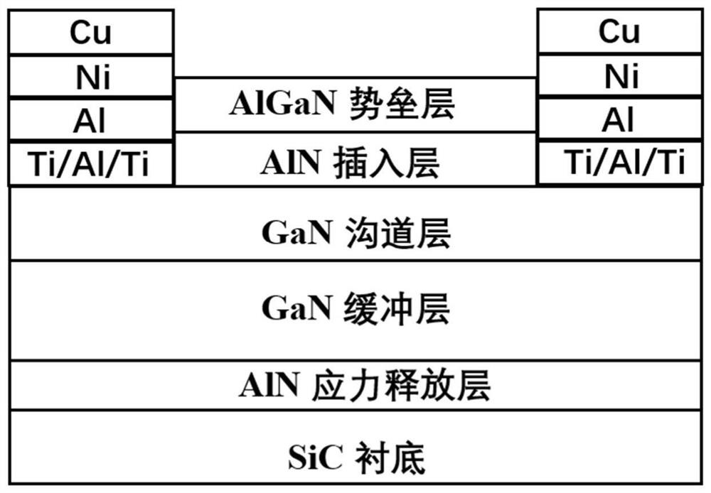
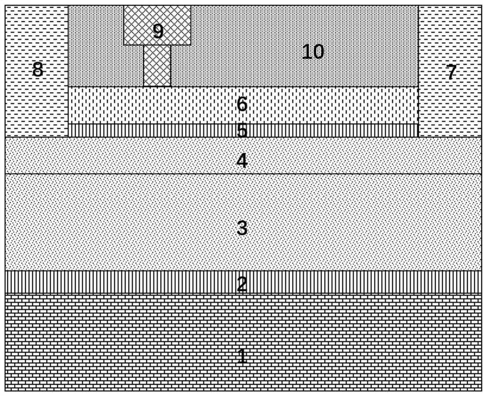
[0025] Next, the technical solutions in the embodiments of the present invention will be clearly and completely described with reference to the accompanying drawings of the present invention, and the described embodiments are only a part of the embodiments of the present invention, rather than all the embodiments. Based on the embodiments of the present invention, other embodiments obtained by persons of ordinary skill in the art without creative work shall fall within the protection scope of the present invention. The experimental methods described in the following examples are conventional methods unless otherwise specified; the reagents and materials can be obtained from open commercial sources unless otherwise specified.

[0026] Spatially relative terms such as "below," "below," "under," "over," "over," "over," and the like are used in this specification to explain the positioning of one element relative to a second element. These terms are intended to encompass different...


PUM

PropertyMeasurementUnit
thicknessaaaaaaaaaa
thicknessaaaaaaaaaa
thicknessaaaaaaaaaa

Abstract

The invention relates to a two-step annealing-based gold-free ohmic contact radio frequency device and a preparation method thereof, and the device comprises a first semiconductor lamination layer which is arranged on a substrate and comprises a nitride channel layer; the source electrode, the second semiconductor lamination layer and the drain electrode are arranged on the first semiconductor lamination layer in the same layer; the second semiconductor lamination layer comprises an insertion layer arranged on the nitride channel layer and a nitride barrier layer arranged on the insertion layer; the grid electrode is arranged on the nitride barrier layer; the source electrode and the drain electrode comprise a contact layer, a covering layer, a barrier layer and a cap layer which are sequentially stacked, the contact layer is formed by circularly stacking a low-work-function metal M sub-layer and a metal Al sub-layer, and the first sub-layer and the last sub-layer are metal M. The annealing alloy temperature is reduced, the problem of high on-resistance is improved, the cut-off frequency and the maximum oscillation frequency of the device are improved, and a process line is prevented from being polluted by formed impurities.

Description

technical field [0001] The invention relates to the field of radio frequency devices, in particular to a radio frequency device without gold ohmic contact based on two-step annealing and a preparation method thereof. Background technique [0002] One of the main problems of current RF power devices is the low dynamic on-resistance, which will reduce the maximum switching frequency of the device and increase the switching loss. Contact metallization schemes for source and drain electrodes have been researched and optimized for more than two decades. To ensure stable, reliable and low-resistance ohmic contact HEMT devices, the most commonly used metal stack scheme is Ti / Al / Ni / Au. From bottom to top are the contact layer, the cover layer, the barrier layer, and the cap layer. Ti is often used as a contact layer, which will react with N in AlGaN to form TiN, resulting in the generation of a large number of N vacancies, which makes electrons prone to tunneling effect. Al is of...

Claims


Application Information

Patent Timeline
Patent Type & Authority Applications(China)
IPC IPC(8): H01L29/778H01L29/45H01L21/335H01L21/28
CPCH01L29/7786H01L29/452H01L29/66462H01L21/28
Inventor 尹以安连梦小
Owner SOUTH CHINA NORMAL UNIVERSITY
Why Eureka
Try Eureka