Display module

A display module and display area technology, which is applied to semiconductor devices, electrical components, circuits, etc., can solve the problems of large width of the lower border area, large occupied border width, and difficulty in realizing narrow borders for OLED display panels, so as to reduce bending Radius, improve bending performance, ensure normal display effect

Pending Publication Date: 2022-07-29
WUHAN CHINA STAR OPTOELECTRONICS SEMICON DISPLAY TECH CO LTD
View PDF0 Cites 0 Cited by
  • Summary
  • Abstract
  • Description
  • Claims
  • Application Information

AI Technical Summary

Problems solved by technology

[0003] Existing OLED display panels include a display area and upper, lower, left, and right frame areas, and the lower frame area generally includes a wiring area and a terminal bending area (pad bending area), and the wiring area is provided with fan-shaped wiring. (fanout routing), VDD routing and VSS routing occupy a large frame width, and the bending radius of the pad bending area has a bending limit, which cannot be further reduced, which leads to a larger width of the lower frame area, making OLED It is difficult for display panels to achieve narrow borders, and this problem needs to be solved urgently

Method used


Image

  • Display module
  • Display module
  • Display module

Examples


Embodiment 1

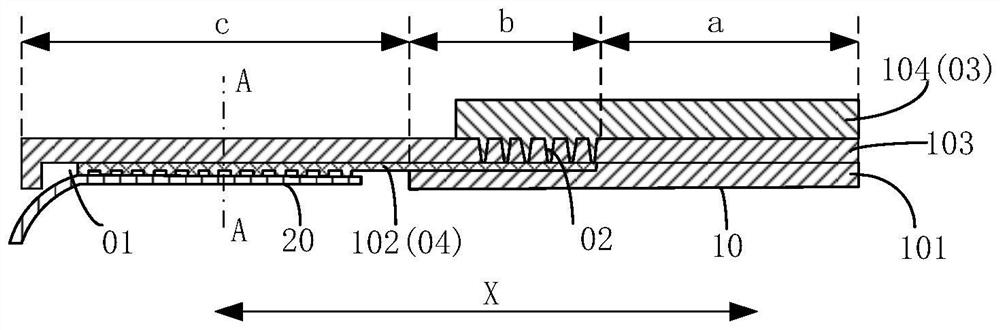
[0025] figure 1 This is a first structural schematic diagram of the display module provided in the first embodiment of the present application. refer to figure 1 , the present application provides a display module, the display module includes a display panel 10, the display panel 10 has a display area a, a bending area c, and a wiring between the display area a and the bending area c Region b, the display panel 10 includes a first substrate 101, a conductive layer 102, a second substrate 103 and a driving circuit layer 104 that are stacked in sequence, wherein the first substrate 101 is in the bending region c A gap 01 is formed, the second substrate 103 is provided with a via hole 02 in the wiring area b, and the driving circuit layer 104 includes a signal line 03 extending from the display area a to the wiring area b , the conductive layer 102 includes a connecting line 04 extending from the bending region c to the routing region b, one end of the connecting line 04 is exp...

Embodiment 2

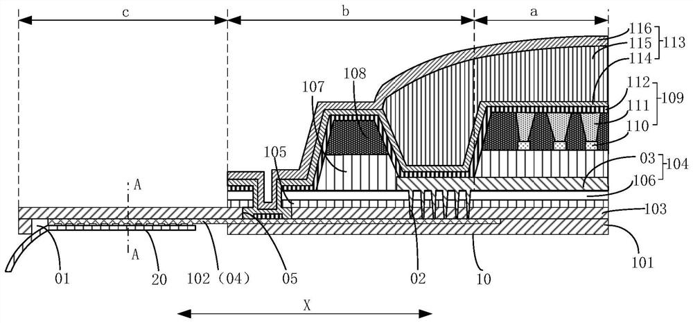
[0044] image 3 A first structural schematic diagram of the display module provided in the second embodiment of the present application; Figure 4 This is a second structural schematic diagram of the display module provided in the second embodiment of the present application. combine image 3 and Figure 4 As shown, the second embodiment of the present application provides a display module, the display module includes a first substrate 101, a conductive layer 102, a second substrate 103, a buffer layer 105, a driving circuit layer 104, The flat layer 107, and the pixel definition layer 108, the pixel unit 109 and the encapsulation layer 113 disposed on the flat layer 107, wherein the first substrate 101 is formed with a notch 01 in the bending region c, the The second substrate 103 is provided with a via hole 02 in the wiring area b, the driving circuit layer 104 includes the signal line 03 extending from the display area a to the wiring area b, and the conductive layer 102...


PUM


Abstract

The invention provides a display module which comprises a display panel, the display panel is provided with a display area, a bending area and a wiring area located between the display area and the bending area, the display panel comprises a first substrate, a conductive layer, a second substrate and a driving circuit layer which are sequentially arranged in a stacked mode, the first substrate is provided with a notch in the bending area, and the first substrate is provided with a first electrode. The second substrate is provided with a via hole in the wiring area, the driving circuit layer comprises a signal line extending from the display area to the wiring area, the conductive layer comprises a connecting line extending from the bending area to the wiring area, one end of the connecting line is exposed by the notch, and the other end of the connecting line is electrically connected with the signal line through the via hole. According to the display panel, the connecting line electrically connected with the signal line is arranged between the two substrates, and the notch for exposing the connecting line is formed in the first substrate in the bending area, so that an external circuit can transmit an electric signal to the display area through the connecting line, the width of a lower frame of the display panel is reduced while the display effect is guaranteed, and the screen-to-body ratio is increased.

Description

technical field [0001] The present application relates to the field of display technology, and in particular, to a display module. Background technique [0002] OLED (Organic Light Emitting Diode, organic light emitting diode, OLED for short) display device has thin, light, wide viewing angle, active light emission, continuously adjustable light emission color, low cost, fast response speed, low energy consumption, low driving voltage and operating temperature. The advantages of wide range, simple production process, high luminous efficiency and flexible display have been listed as the next generation display technology with great development prospects. [0003] The existing OLED display panel includes a display area and upper, lower, left and right frame areas, and the lower frame area generally includes a wiring area and a pad bending area, and the wiring area is provided with fan-shaped wirings (fanout traces), VDD traces and VSS traces occupy a large width of the frame,...

Claims


Application Information

Patent Timeline
Patent Type & Authority Applications(China)
IPC IPC(8): H01L27/32
CPCH10K59/131
Inventor 李强刘汉辰鲜于文旭江应传张春鹏
Owner WUHAN CHINA STAR OPTOELECTRONICS SEMICON DISPLAY TECH CO LTD
Why Eureka
Try Eureka