Transfer method of LED chip and display panel
A technology of LED chip and transfer method, which is applied in the manufacture of semiconductor devices, electrical components, semiconductor/solid-state devices, etc., can solve the problems of low transfer efficiency, low yield rate, and virtual soldering, and achieve improved yield rate, reduced ratio of virtual soldering, Effect of Improving Transfer Efficiency
- Summary
- Abstract
- Description
- Claims
- Application Information
AI Technical Summary
Problems solved by technology
Method used
Image

Examples
Embodiment Construction
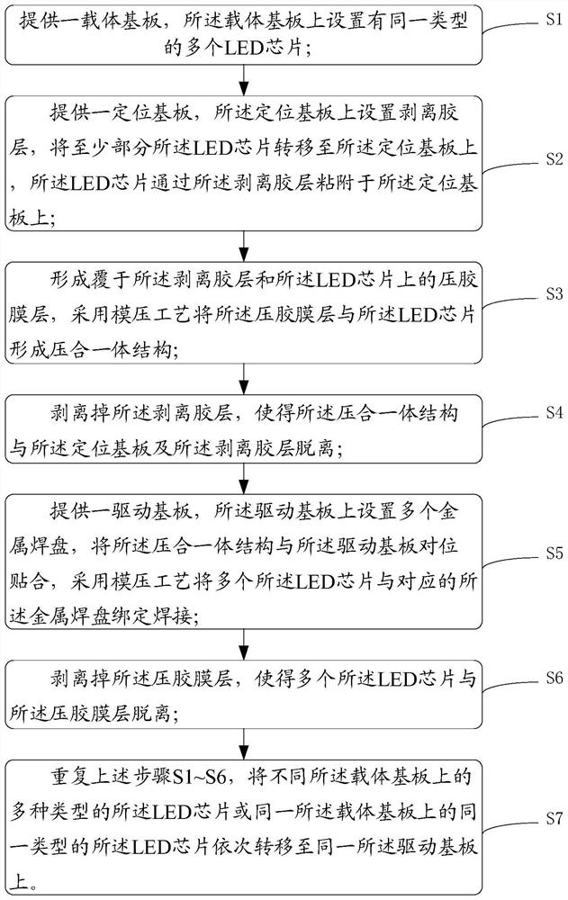
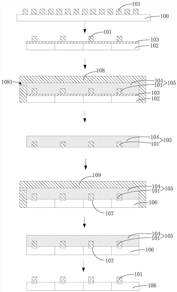
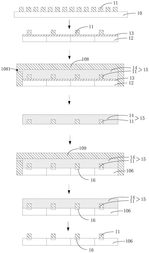
[0043] The technical solutions in the embodiments of the present invention will be clearly and completely described below with reference to the accompanying drawings in the embodiments of the present invention. Obviously, the described embodiments are only a part of the embodiments of the present invention, rather than all the embodiments. Based on the embodiments of the present invention, all other embodiments obtained by those skilled in the art without creative efforts shall fall within the protection scope of the present invention. In addition, it should be understood that the specific embodiments described herein are only used to illustrate and explain the present invention, but not to limit the present invention. In the present invention, unless otherwise stated, the directional words such as "upper" and "lower" generally refer to the upper and lower parts of the device in actual use or working state, specifically the direction of the drawing in the accompanying drawings....
PUM
 Abstract
Description
Claims
Application Information
 - R&D Engineer
- R&D Manager
- IP Professional
- Industry Leading Data Capabilities
- Powerful AI technology
- Patent DNA Extraction
Browse by: Latest US Patents, China's latest patents, Technical Efficacy Thesaurus, Application Domain, Technology Topic.
© 2024 PatSnap. All rights reserved.Legal|Privacy policy|Modern Slavery Act Transparency Statement|Sitemap