Electronic component production die bonding equipment and use method thereof

A technology for electronic components and crystal bonding, which is applied in the field of crystal bonding equipment for the production of electronic components. It can solve the problems of not being able to fix multiple chips, waste, and insufficient amount of bonding glue, and achieve the effect of improving the baking effect and efficiency.

Active Publication Date: 2022-08-05
江苏丰源电子科技有限公司
View PDF5 Cites 0 Cited by
  • Summary
  • Abstract
  • Description
  • Claims
  • Application Information

AI Technical Summary

Problems solved by technology

[0003] In the production process of electronic components, die-bonding equipment needs to be used. The existing die-bonding equipment needs to apply the die-bonding glue on the substrate during work, and then fix the chip in the dispensing area, so that the chip and the substrate are fixed, but directly Applying the die-bonding glue on the substrate, for chips of different sizes, there will be two situations: the insufficient amount of the die-bonding glue will cause the fixing effect to be unstable or the excess of the die-bonding glue will cause waste. Fix multiple chips on the same substrate, the existing die bonding equipment cannot fix multiple chips at the same time, so the efficiency of die bonding is low

Method used


Image

  • Electronic component production die bonding equipment and use method thereof
  • Electronic component production die bonding equipment and use method thereof
  • Electronic component production die bonding equipment and use method thereof

Examples


Embodiment Construction

[0034] Embodiments of the present invention are described in detail below with reference to the accompanying drawings, but the present invention can be implemented in many different ways as defined and covered by the claims.

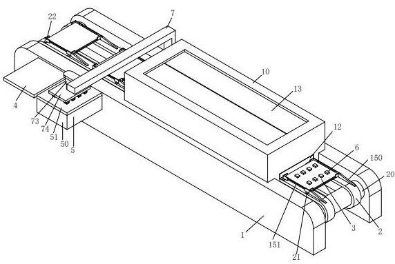
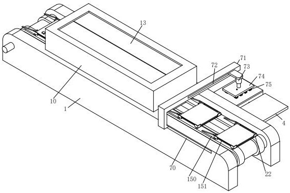
[0035] see figure 1 , an electronic component production die-bonding equipment, comprising two support tables 1, a conveyor 2 for conveying a substrate 3 is installed between the two support tables 1, and one of the support tables 1 is installed on the end face away from the conveyor 2 along The placing table 4 and the plastic box 5 are arranged in sequence in the conveying direction of the conveyor 2. The placing table 4 is used to place the wafer 6, the plastic box 5 is used to store the die-bonding glue, and another support table 1 is installed on the other support table 1 to suck and fix the wafer 6. The drive assembly 7.

[0036] see figure 1 and figure 2, the conveyor 2 is composed of two conveyor rollers 20 and two conveyor belts, the two conv...


PUM


Abstract

The invention relates to the technical field of die bonding, in particular to electronic component production die bonding equipment and a use method thereof, the electronic component production die bonding equipment comprises two supporting tables, a conveyor for conveying a substrate is mounted between the two supporting tables, and a placement table and a glue box which are sequentially arranged in the conveying direction of the conveyor are mounted on the end face, away from the conveyor, of one supporting table. According to the die bonding equipment for electronic component production, a plurality of wafers can be fixed on the substrate at the same time, and the die bonding glue in the charging hopper is shaken and stirred in the process of coating the wafers with the die bonding glue, so that the problem of poor fixing effect between the wafers and the substrate caused by solidification of the die bonding glue is prevented; and the bottoms of a plurality of wafers are simultaneously inserted into the inserting and coating through grooves for gluing, so that not only can the die bonding efficiency of the electronic element be improved, but also the problem of waste of the die bonding glue caused by directly coating more die bonding glue on the substrate is avoided.

Description

technical field [0001] The invention relates to the technical field of die bonding, in particular to a die bonding device for producing electronic components and a method for using the same. Background technique [0002] Electronic components are the basic elements in electronic circuits. They are usually individual packages and have two or more leads or metal contacts. Electronic components must be connected to each other to form an electronic circuit with a specific function. [0003] In the production process of electronic components, a die-bonding equipment is required. The existing die-bonding equipment needs to apply the die-bonding glue on the substrate during operation, and then fix the wafer in the dispensing area, so that the wafer and the substrate are fixed, but directly. When the die-bonding glue is applied to the substrate, for wafers of different sizes, there are two situations: insufficient amount of die-bonding glue leads to unstable fixing effect or too muc...

Claims


Application Information

Patent Timeline
Patent Type & Authority Applications(China)
IPC IPC(8): H01L21/67H01L21/60
CPCH01L21/67144H01L21/60H01L2021/60277
Inventor 郑石磊
Owner 江苏丰源电子科技有限公司
Why Eureka
Try Eureka