Method for forming integrated circuit

A technology of integrated circuits and conductive layers, applied in circuits, electrical components, electrical solid devices, etc., can solve problems such as harmful effects of fuse windows

Inactive Publication Date: 2004-08-04
FREESCALE SEMICON INC
View PDF0 Cites 0 Cited by
  • Summary
  • Abstract
  • Description
  • Claims
  • Application Information

AI Technical Summary

Problems solved by technology

However, removal of the TiN anti-reflective coating can have detrimental e...

Method used


Image

  • Method for forming integrated circuit
  • Method for forming integrated circuit
  • Method for forming integrated circuit

Examples


Embodiment Construction

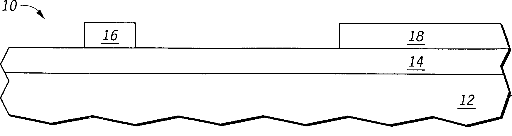
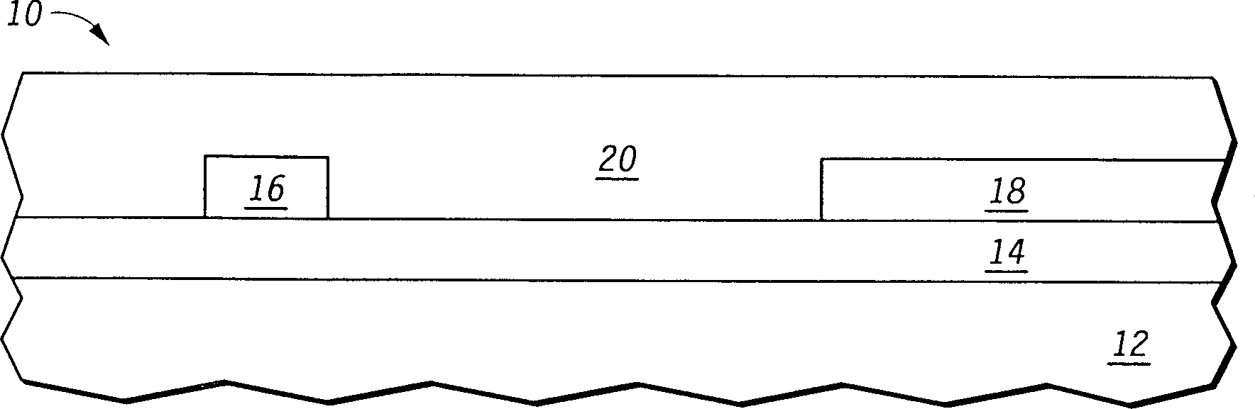
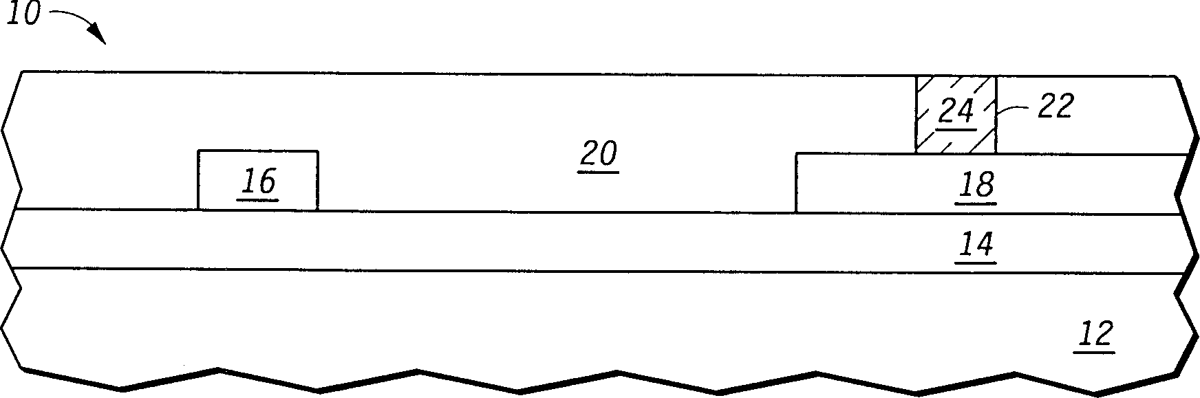
[0008] Figure 1-7 Cross-sectional views illustrating process steps of forming an integrated circuit in accordance with one embodiment of the present invention. figure 1 is a portion 10 of an integrated circuit structure that includes a semiconductor substrate 12 , a dielectric layer 14 , fuses 16 , and conductive interconnects 18 . In one embodiment, semiconductor substrate 12 is a single crystal silicon substrate. In addition, the semiconductor substrate 12 may also be a silicon-on-insulator substrate, a silicon-on-sapphire substrate, or the like.

[0009] In one embodiment, the dielectric layer 14 is a plasma deposited oxide layer formed using tetraethyl orthosilicate (TEOS) as a gas source. In addition, the dielectric layer 14 can be a silicon nitride layer, a phosphosilicate glass (PSG) layer, a borophosphosilicate glass (BPSG) layer, a spin-on glass (SOG) layer, a silicon oxynitride layer, a polyimide layer, a low dielectric Electrical constant insulators, or a combin...


PUM


Abstract

In one embodiment, a first dielectric layer (32) that overlies a fuse (16) and a bonding pad (30) is etched with a first etch process. This first etch process exposes a portion (40) of a second dielectric layer (20) that underlies the first dielectric layer (32) and overlies the fuse (16). In addition, the first etch process also forms a bond pad opening (38) that exposes a portion (42) of an anti-reflective layer (28) that forms a portion of the bonding pad (30). A second etch process is then used to etch the exposed portion (42) of the anti-reflective layer (28) and the exposed portion (40) of the second dielectric layer (20) at substantially the same rate to form a fuse window (45) overlying the fuse (16). The second etch process prevents over etching of the second dielectric layer (20), and thus exposure of the underlying fuse (16).

Description

technical field [0001] The present invention relates generally to integrated circuits, and more particularly to methods of forming fuse windows and bond pad holes in integrated circuits. Background technique [0002] The semiconductor industry has led to ever-increasing lithographic patterning problems with the widespread use of highly reflective interconnect materials such as polysilicon, aluminum, refractory metals, and metal silicides to progressively shrink integrated circuit geometries. Unwanted reflections from underlying interconnect material during photoresist patterning cause distortions in the interconnect photoresist pattern and the resulting interconnect. This problem is compounded when photolithographic patterning tools with UV and deep UV exposure wavelengths are used to generate photoresist patterns. [0003] One process suggested to minimize reflections from underlying reflective interconnect material is to form an anti-reflective coating on the photoresist ...

Claims


Application Information

Patent Timeline
IPC IPC(8): H01L21/82H01L23/485H01L23/525
CPCH01L2924/01015H01L2924/01082H01L2924/01004H01L24/05H01L23/5258H01L2224/05624H01L23/53228H01L2924/01002H01L2924/01029H01L2924/01022H01L2224/02166H01L2924/01013H01L23/53214H01L24/03H01L2924/05042H01L2924/04941H01L2924/01007H01L2924/14H01L2224/05647H01L2924/01005H01L2924/01033H01L2924/01006H01L2924/01074H01L2924/01078H01L2924/01014H01L2924/00014H01L27/00
Inventor 卡尔·L·鲍恩凯思·Q·劳
Owner FREESCALE SEMICON INC
Why Eureka
Try Eureka