Semiconductor integrated circuit device capable of inhibiting noise and supplying power potential

A technology of integrated circuits and semiconductors, applied in the fields of semiconductor devices, semiconductor/solid-state device manufacturing, circuits, etc., can solve problems such as difficult supply and high voltage, and achieve the effect of suppressing the increase of chip area

Inactive Publication Date: 2004-12-29
MITSUBISHI ELECTRIC CORP
View PDF0 Cites 0 Cited by
  • Summary
  • Abstract
  • Description
  • Claims
  • Application Information

AI Technical Summary

Problems solved by technology

[0032] In addition, in the test mode, when the potential is supplied from the outside to the internal circuit through the terminal 8020, it is difficult to supply a very high voltage to the internal circuit due to the withstand voltage limit of the transistor.

Method used


Image

  • Semiconductor integrated circuit device capable of inhibiting noise and supplying power potential
  • Semiconductor integrated circuit device capable of inhibiting noise and supplying power potential
  • Semiconductor integrated circuit device capable of inhibiting noise and supplying power potential

Examples


Embodiment 2

[0097] FIG. 6 is a circuit diagram showing the configuration of a coupling circuit 2102 mounted in the semiconductor memory device according to Embodiment 2 of the present invention.

[0098] The structure of the other parts of the semiconductor storage device of the second embodiment is the same as that of the semiconductor storage device of the first embodiment, and therefore description thereof will not be repeated.

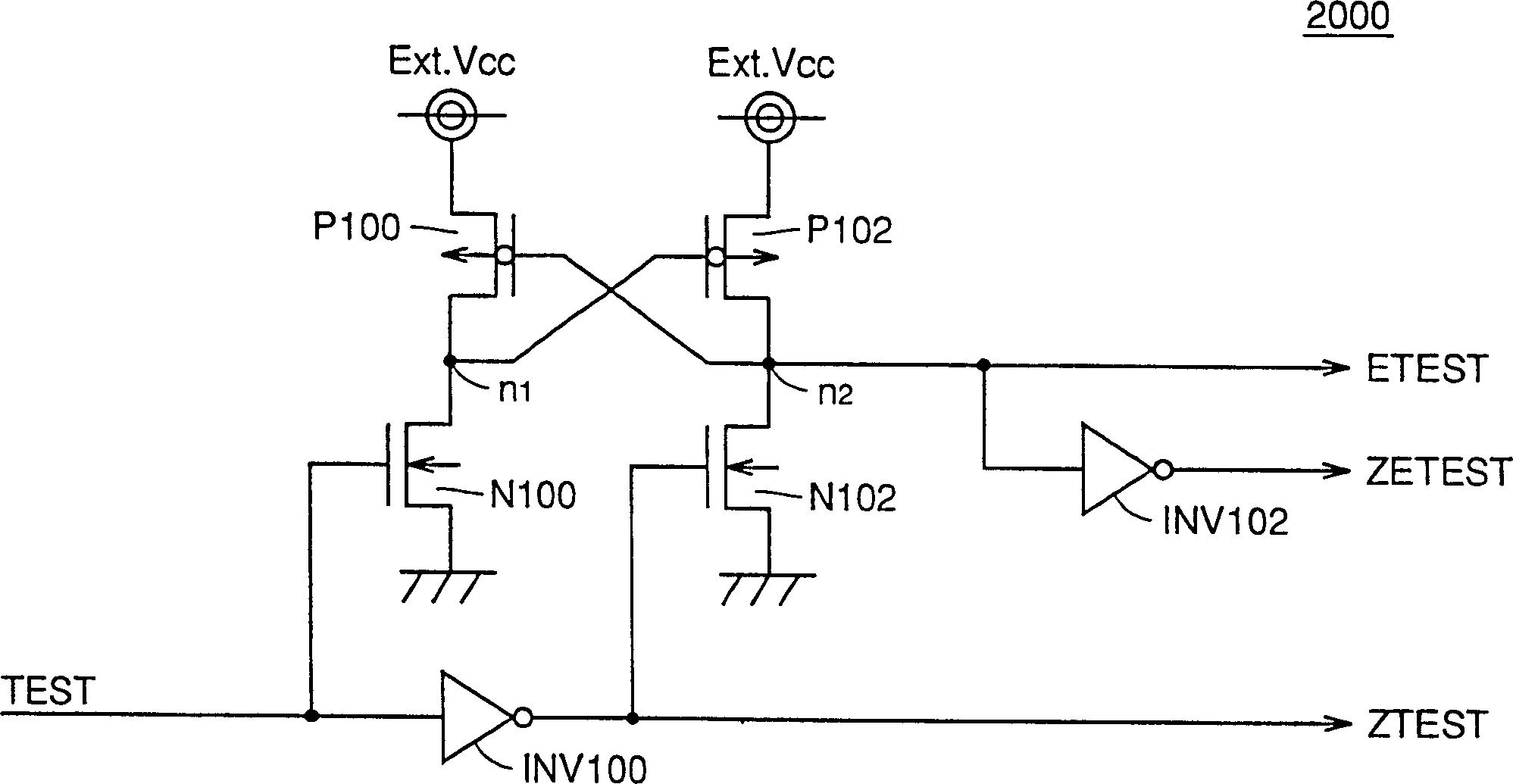
[0099] Referring to FIG. 6, the coupling circuit 2102 has P-channel MOS transistors P212 and P214 connected in series between the terminal 118 and the internal power supply node ns1 (and ns2), and a gate potential coupled between the terminal 118 and the gate of the transistor P212. The P-channel MOS transistor 210 controlled by the signal TEST and the N-channel MOS transistor N210 coupled between the ground potential GND and the gate potential of the transistor P212 is controlled by the signal ETEST. The gate potential of the transistor P214 provided on the i...

Embodiment 3

[0112] FIG. 7 is a circuit diagram showing the configuration of a coupling circuit 2104 mounted in the semiconductor memory device according to Embodiment 3 of the present invention.

[0113] The structure of the other parts of the semiconductor storage device of the third embodiment is the same as that of the semiconductor storage device of the first embodiment, and therefore description thereof will not be repeated.

[0114] Referring to FIG. 7, the coupling circuit 2104 has N-channel MOS transistors N112 and N114 connected in series between the terminal 118 and the internal power supply node ns1 (and ns2), and a gate potential coupled between the terminal 118 and the gate of the transistor N112. An N-channel MOS transistor N110 controlled by a signal ZTEST, and a P-channel MOS transistor P110 whose gate potential is controlled by a signal ZETEST is coupled between the external power supply potential Ext. Vcc and the gate of the transistor N112. The gate potential of the tra...


PUM


Abstract

An external terminal and an internal power supply node to an internal circuit are connected via first and second transistors. In a test operation mode, the first and second transisters are turned on and potential is accordingly supplied to the internal circuit from the terminal. In a normal operation mode, a third transistor placed between the terminal and the gate of the first transistor is turned on so that the gate of the first transistor is coupled to the external terminal and the second transistor is turned off. Undershoot to the terminal is not transmitted to the inside since the first transistor is turned off.

Description

technical field [0001] The present invention relates to a structure for supplying a power supply potential to an internal circuit in a test operation mode of a semiconductor integrated circuit device. More specifically, the present invention relates to a semiconductor integrated circuit device having a power supply circuit for supplying an arbitrary voltage supplied from the outside to an internal circuit during a test mode operation. Background technique [0002] With the improvement of the integration level of semiconductor memory such as dynamic random access memory (hereinafter referred to as DRAM), the semiconductor integrated circuit device must ensure the reliability of the miniaturized transistors constituting the circuit. Requirements such as interface specifications for external data transmission and reception of semiconductor integrated circuits. [0003] Therefore, a step-down power supply circuit that steps down an external power supply potential Ext. Vcc to ge...

Claims


Application Information

Patent Timeline
Patent Type & Authority Patents(China)
IPC IPC(8): G11C11/407G11C5/14G11C11/401G11C29/06G11C29/12G11C29/50H01L21/822H01L27/04
CPCG11C5/147G11C29/12G11C5/14G11C11/404
Inventor 松本康宽赤松宏
Owner MITSUBISHI ELECTRIC CORP
Why Eureka
Try Eureka