Supercharge Your Innovation With Domain-Expert AI Agents!

Output buffering device and method

An output device, output buffer technology, applied in pulse technology, logic circuit connection/interface layout, electrical components, etc., can solve problems such as increased noise and distortion

Inactive Publication Date: 2005-05-04
SAMSUNG ELECTRONICS CO LTD
View PDF0 Cites 0 Cited by
  • Summary
  • Abstract
  • Description
  • Claims
  • Application Information

AI Technical Summary

Problems solved by technology

In this way, the noise and distortion in the buffered signal OUT due to the bouncing of the ground voltage and the impedance mismatch between the output port 20 and the output buffer 10 are also increased.

Method used


Image

  • Output buffering device and method
  • Output buffering device and method
  • Output buffering device and method

Examples


Embodiment Construction

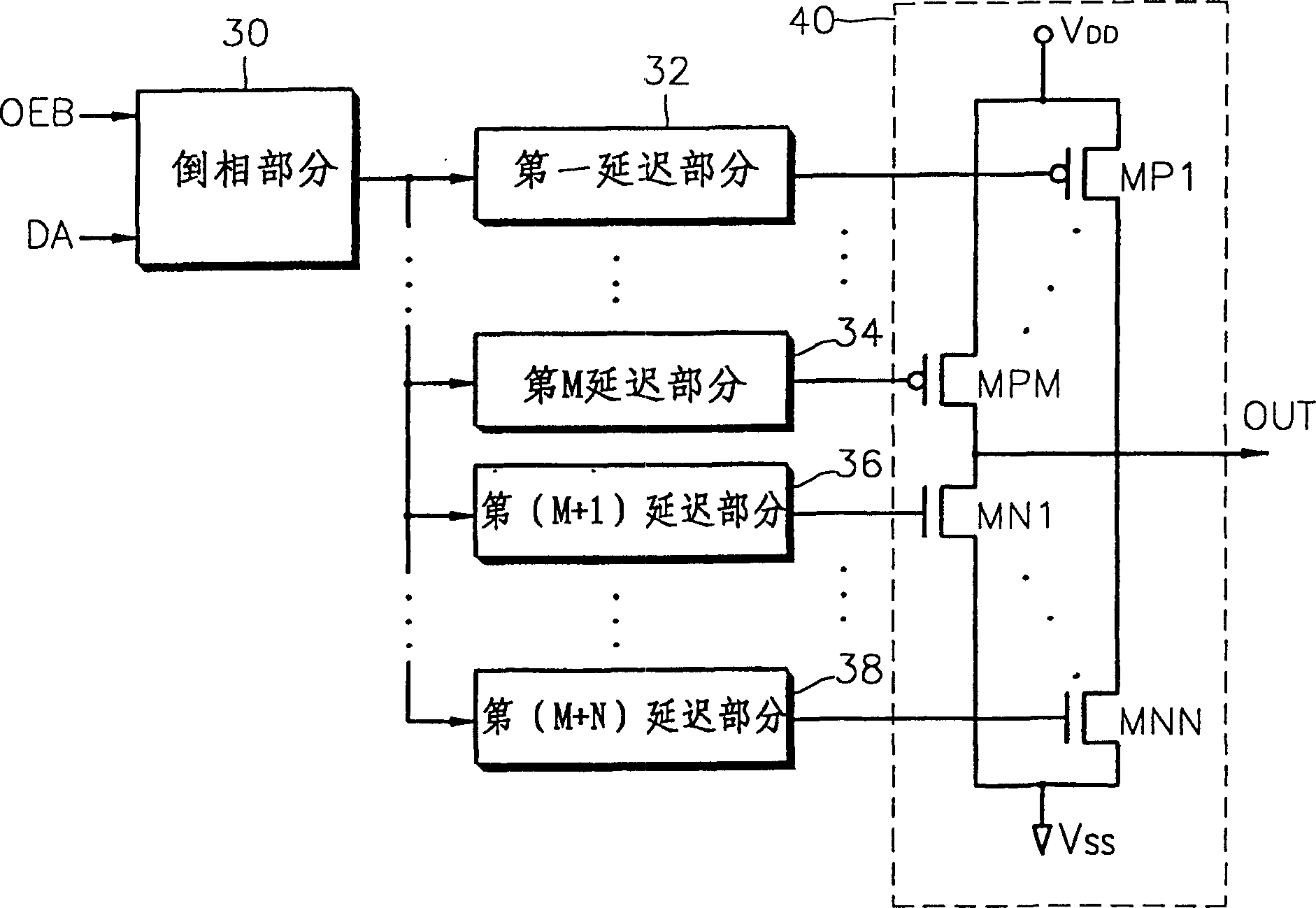
[0033] Depend on figure 2 It can be seen that the output buffer constituted by a preferred embodiment of the present invention includes an inverting part 30, first to M delay parts 32 to 34, (M+1) to (M+N) delay parts 36 to 38 , and a data output part 40 composed of first to Mth pull-up transistors MP1 to MPM and first to Nth pull-down transistors MN1 to MNN.

[0034] figure 2The inverting part 30 shown in inverts the input data DA and outputs it to the first to Mth delay parts 32 to 34 and the (M+1) to (M+N) delay parts 36 to 38 (wherein M and N each is a positive integer equal to or greater than 2). The inverting part 30 works under the action of the output enable signal OEB to invert the input data DA. The first to M delay sections 32 to 34 and the (M+1) to (M+N) delay sections 36 to 38 delay the inverted input data for M+N different delay times every T / ( M+N) times are sent to the data output section 40 one by one (where T is the time required for the level change of...


PUM


Abstract

The invention discloses an output buffer capable of reducing noise and distortion of buffered input data during high-speed operation and a buffering method implemented in the output buffer. The output buffer is used to buffer the input data and output the buffered input data as output data, the output buffer includes: first to Mth and (M+1) to (M+N)th delays means for delaying input data by (M+N) different delay times, and outputting the delayed data at intervals of T / (M+N) in a predetermined order, where M and N are each equal to or greater than 2 and T corresponds to the time required to change the level of the output data; and data output means for outputting data in response to outputs of the first to (M+N)th delay means.

Description

technical field [0001] The present invention relates to output buffers and methods of output buffering, and more particularly to output buffers usable in integrated circuits. Background technique [0002] Traditional output buffers are described in many textbooks. For example, in "CMOS VLSI Design Principles - A Systems Perspective," by Nail Weste and Kamran Eshraghian, "Addison Wesley" Publishing Company, 1985, pp. 229-230 at Figure 5-6 1 shows a conventional output buffer. [0003] The conventional output buffer shown in FIG. 1 includes an output buffer 10 and an output port 20 . The output buffer 10 includes an inverter 12, a NAND gate 14, a NOR gate 16, and PMOS and NMOS transistors MPO and MNO. [0004] The output buffer 10 for an integrated circuit of FIG. 1 delays input data DA having a logic "high" or "low" level for a predetermined time and sends it to an output port 20. The output buffer 10 is built in an integrated circuit. Normally, the output buffer 10 is e...

Claims


Application Information

Patent Timeline
Patent Type & Authority Patents(China)
IPC IPC(8): H03K19/0175H03K17/16H03K19/00
CPCH03K17/164H03K19/00
Inventor 韩秉勋安秉权
Owner SAMSUNG ELECTRONICS CO LTD
Features
  • R&D
  • Intellectual Property
  • Life Sciences
  • Materials
  • Tech Scout
  • Unparalleled Data Quality
  • Higher Quality Content
  • 60% Fewer Hallucinations
Learn More