

Preparation method of tunnelling oxidized layer in imbedded type quick flash storage
A technology for tunneling oxide layer and memory, applied in semiconductor/solid-state device manufacturing, electrical components, circuits, etc., can solve the problems of tunnel oxide layer thickness limitation, affecting device reliability, unrealistic process technology, etc.
- Summary
- Abstract
- Description
- Claims
- Application Information
AI Technical Summary
Problems solved by technology
Method used
Image

Examples
Embodiment Construction
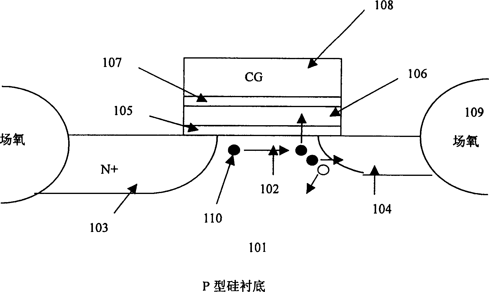
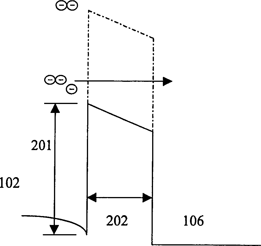
[0017] see figure 1 As shown, a method for preparing a tunnel oxide layer in an embedded flash memory of the present invention is characterized in that the method includes the following steps,
[0018] 1) First, the silicon wafer 101 on which the tunneling oxide layer 105 is to be grown is cleaned, and the cleaning solution is No. 1 cleaning solution and No. 2 cleaning solution (which is the prior art);
[0019] 2) Then use a dry etching machine to carry out fluorination treatment on a dry etching machine, under a pressure of 500mTorr, pass 100SCCM CF 4 Gas flow rate, the gap height between the upper and lower electrodes of the dry etching machine is 1.1cm, the power is 10W, and the time is 1-2 minutes;
[0020] 3) After the treatment, the silicon wafer 101 is cleaned conventionally, and then cleaned in isopropanol cleaning solution for 1 minute;
[0021] 4) Send the silicon wafer 101 into a high-temperature oxidation furnace for treatment, which is to oxidize at 850° C. for...
PUM
 Abstract
Description
Claims
Application Information