Plasma processing apparatus

A plasma and processing device technology, applied in the field of plasma processing devices, can solve the problems of the influence of the good rate of the manufacturing process, the damage of the ceramic cover, the damage of the equipment parts, etc.

Inactive Publication Date: 2005-11-30
AU OPTRONICS CORP
View PDF0 Cites 0 Cited by
  • Summary
  • Abstract
  • Description
  • Claims
  • Application Information

AI Technical Summary

Problems solved by technology

Under the continuous bombardment of the plasma, the exposed aluminum material will fall onto the product (glass), resulting in defects, and the good rate is seriously lost
In addition, after the surface of the anodized aluminum film at the air hole 16 is peeled off, the ceramic cover plate 14 covered on it is indirectly damaged. This accident often causes serious damage to equipment parts, and has a more serious impact on the good rate of the manufacturing process.

Method used


Image

  • Plasma processing apparatus
  • Plasma processing apparatus
  • Plasma processing apparatus

Examples


Embodiment Construction

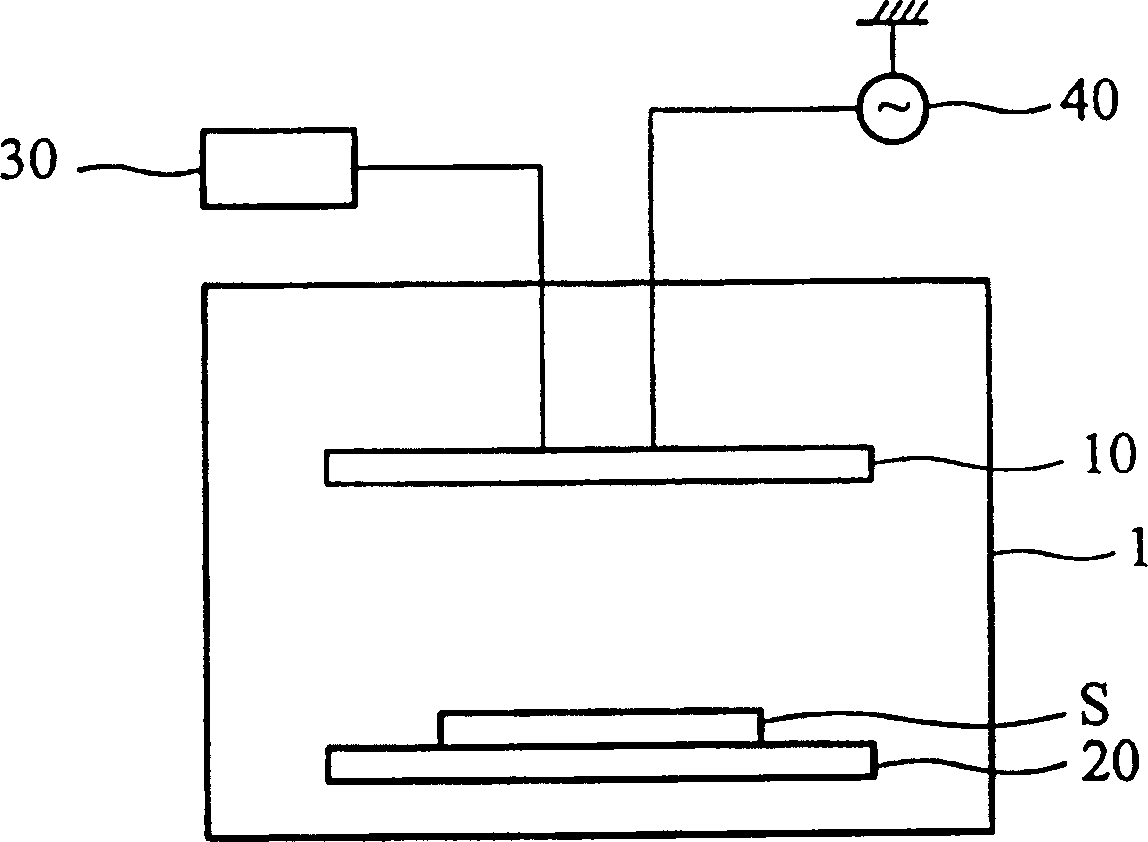
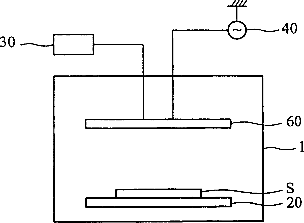
[0024] image 3 A schematic diagram showing a plasma processing apparatus according to a preferred embodiment of the present invention. The plasma processing device includes a processing chamber 1 , a gas supply system 30 and a power source 40 . Inside the processing chamber 1 , there is an upper electrode plate 60 and a lower electrode plate 20 . A substrate S to be subjected to plasma treatment can be placed on the lower electrode plate 20, such as a semiconductor substrate used in the semiconductor manufacturing process, or a glass substrate or transparent plastic substrate used in the TFT-LCD manufacturing process. The gas supply system 30 can supply gas into the processing chamber 1 . The power source 40 may be a radio frequency (RF) for applying a voltage difference between the upper and lower electrode plates 60 and 20 to convert the gas in the processing chamber 1 into plasma.

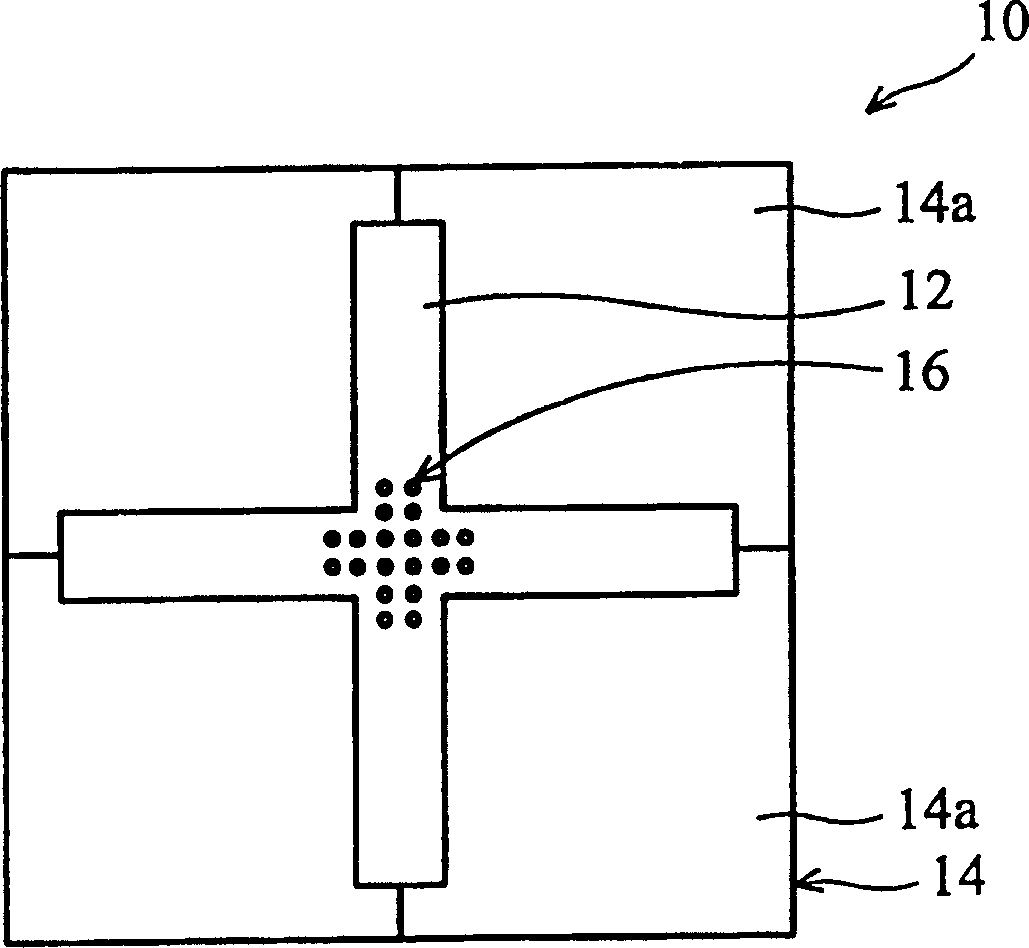
[0025] A feature of the present invention is the improvement of the upper electrode plat...


PUM


Abstract

The invention provides a plasma processing unit, wherein the upper plate electrode comprises an insulating cover plate and a supporting frame mounted on the bottom of the insulating cover plate to support the insulating cover plate, it also has a hole, and gas demarcation strip constructed through insulating material. The unit is mounted in the hole for supporting the frame. The invention can eliminate product defects and increase quality ratio.

Description

technical field [0001] The invention relates to a plasma processing device, in particular to a plasma processing device which can avoid arc discharge. Background technique [0002] In the TFT-LCD front-end array (array) manufacturing process, it is often necessary to use a plasma processing device for etching and deposition. For example, etching of an amorphous silicon layer or a polysilicon layer in a TFT is performed using a plasma processing apparatus. [0003] figure 1 A schematic diagram of a conventional plasma processing device is shown, which includes a processing chamber 1 with an upper electrode plate 10 and a lower electrode plate 20 inside the chamber 1 . A gas supply system 30 and a power source 40 are connected to the upper electrode plate 10, and the power source 40 may be radio frequency (radio frequency RF). The gas supply system 30 can supply gas into the cavity 1 , and the radio frequency is used to provide a voltage difference between the upper and low...

Claims


Application Information

Patent Timeline
Patent Type & Authority Patents(China)
IPC IPC(8): C23F1/00G02F1/13H01J37/36H01L21/203H01L21/3065H01L21/363H01L21/465H05H1/46
Inventor 李孝忠黄庆德戴嘉宏陈虹瑞赖宏裕
Owner AU OPTRONICS CORP
Why Eureka
Try Eureka