Method for mfg. high voltage element

A technology of high-voltage components and manufacturing methods, which is applied in the manufacture of semiconductor/solid-state devices, electrical components, circuits, etc., can solve the problem that the breakdown voltage of high-voltage components cannot be effectively increased, and achieve the effect of increasing the value of the breakdown voltage

Inactive Publication Date: 2006-06-21
MACRONIX INT CO LTD
View PDF0 Cites 0 Cited by
  • Summary
  • Abstract
  • Description
  • Claims
  • Application Information

AI Technical Summary

Problems solved by technology

In this way, the breakdown voltage of high-voltage components will not be effectively improved

Method used


Image

  • Method for mfg. high voltage element
  • Method for mfg. high voltage element
  • Method for mfg. high voltage element

Examples


Embodiment Construction

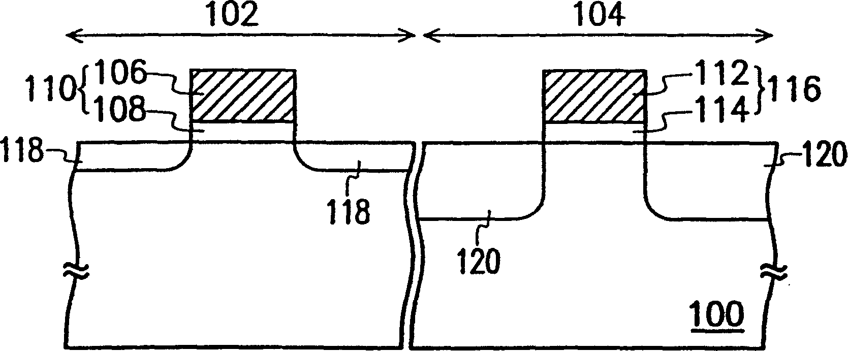
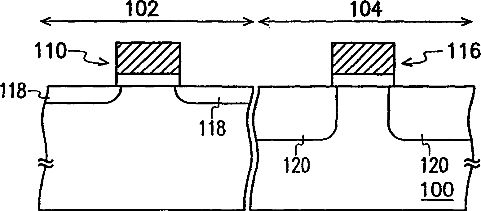
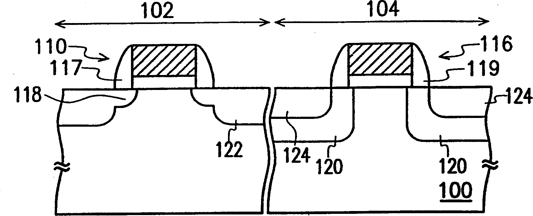
[0029] Figure 2A to Figure 2E , which is a schematic cross-sectional view of the manufacturing process of a high-voltage element according to a preferred embodiment of the present invention.

[0030] Please refer to Figure 2A Firstly, a substrate 200 is provided, wherein the substrate 200 has a general device region 202 and a high voltage device region 204 . Next, a gate structure 210 and 216 are respectively formed on the normal device region 202 and the high voltage device region. Wherein, the gate structure 210 , 216 includes a gate conductive layer 206 , 212 and a gate oxide layer 208 , 214 . The material of the gate conductive layers 210 and 216 is, for example, polysilicon.

[0031] After that, please refer to Figure 2B A lightly doped drain region (LDD) 218 ​​is formed in the substrate 200 on both sides of the gate structure 210 in the general device region 202 . Next, a first thermal process is performed. The first thermal process is a tempering step performed...


PUM


Abstract

A manufacturing method of a high-voltage element, which firstly provides a substrate, wherein a gate structure of a high-voltage element has been formed on the substrate. Then, after the first thermal process is performed, a first doped region is formed in the substrate on both sides of the gate structure of the high voltage element. Afterwards, a spacer is formed on the side of the gate structure of the high voltage device. And an oxide layer is formed on the gate structure of the high voltage element and on the surface of the first doped region. Then, after performing a second thermal process, a second doped region is formed in the substrate on both sides of the spacer.

Description

technical field [0001] The present invention relates to a manufacturing method of a semiconductor device, and in particular to a manufacturing method of a high voltage device (High Voltage Device). Background technique [0002] High-voltage components, as the name suggests, are components that can withstand higher bias voltages, which means that the breakdown voltage of high-voltage components will be higher than that of ordinary components. High voltage components are generally preferred in nature by having a higher breakdown voltage. In addition, high voltage components are often fabricated on the same chip along with general components. A typical structure of a high voltage device includes a gate, a source / drain region and a lightly doped drain (LDD). Wherein, the lightly doped drain region of the high voltage element surrounds the source / drain region. [0003] Figure 1A to Figure 1D As shown in FIG. 1 , it is a schematic cross-sectional view of a manufacturing proces...

Claims


Application Information

Patent Timeline
Patent Type & Authority Patents(China)
IPC IPC(8): H01L21/336H01L21/265H01L21/324
Inventor 刘慕义范左鸿叶彦宏詹光阳卢道政
Owner MACRONIX INT CO LTD
Why Eureka
Try Eureka