A heterojunction device with integrated diode

A heterojunction and diode technology, applied in semiconductor devices, electrical components, circuits, etc., can solve problems such as ineffective energy consumption, no parasitic diode structure, and component failure, so as to improve the overall performance of the device and increase the concentration of 2DEG Effect

Inactive Publication Date: 2018-02-06
SOUTHWEST JIAOTONG UNIV
View PDF2 Cites 0 Cited by
  • Summary
  • Abstract
  • Description
  • Claims
  • Application Information

AI Technical Summary

Problems solved by technology

However, compound semiconductor field effect transistor devices such as GaN-HFET usually do not have a P region and therefore do not have a parasitic diode structure, so the energy from the inductive load cannot be effectively dissipated within the element. When the energy exceeds the gate-drain withstand voltage region, When the source-drain cut-off withstand voltage will cause component failure

Method used


Image

  • A heterojunction device with integrated diode
  • A heterojunction device with integrated diode
  • A heterojunction device with integrated diode

Examples


Embodiment 1

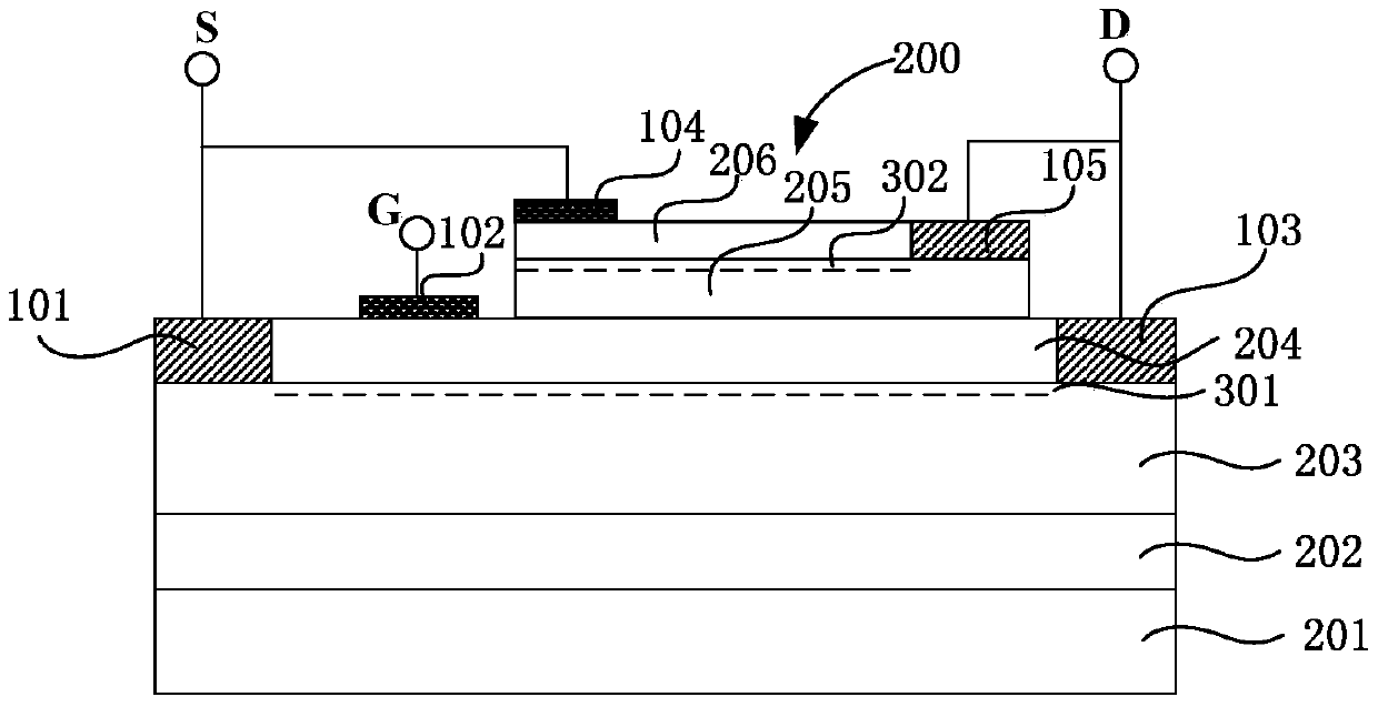
[0040] figure 1 It shows a heterojunction device with an integrated diode in this embodiment, including a second semiconductor buffer layer 202, a third semiconductor layer 203, and a fourth semiconductor layer 204 sequentially deposited on a first semiconductor substrate layer 201; The semiconductor layer 203 and the fourth semiconductor layer 204 can form a heterojunction, and the first conductive channel 301 is on the heterojunction interface; the two ends of the fourth semiconductor layer 204 are respectively provided with a first ohmic contact 101 and a second ohmic contact 103; The first metal electrode 102 and the heterojunction diode 200 are disposed on the fourth semiconductor 204 between the first ohmic contact 101 and the second ohmic contact 103 .

[0041] The first ohmic contact 101, the second ohmic contact 103, the metal electrode 102 and the first conductive channel 301 constitute a heterojunction MISHFET, and the electrode of the first ohmic contact 101 serves...

Embodiment 2

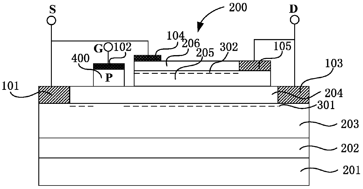
[0049] figure 2 A heterojunction device with integrated diodes of this embodiment is shown. This embodiment is a derivative structure of Embodiment 1. The difference from Embodiment 1 will be described below. The gate 102 and the fourth semiconductor layer 204 are provided with a first doped layer 400, and the first doped layer 400 is a P-type doped layer, and the material used is P-type Si 3 N 4 、SiN x , HfO 2 , Ga 2 o 3 , CrO, AlN, SiO 2 、Al 2 o 3 、TiO 2 , MgO, MnO and multi-element compound insulating material AlHfO x 1, HfSiON or a composite layer of several materials; the implementation principle of the heterojunction device in Example 2 is the same as that in Example 1, and will not be repeated here.

Embodiment 3

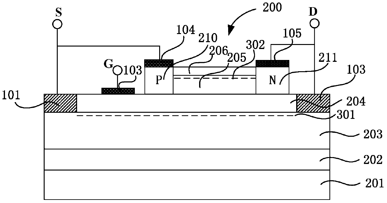
[0051] image 3A heterojunction device with integrated diodes of the present implementation is shown. The heterojunction diode 200 in this embodiment includes a tenth semiconductor layer 210, an eleventh semiconductor layer 211 deposited on the fourth semiconductor 204, a fifth semiconductor layer 205 and a sixth semiconductor layer 206 arranged in sequence from bottom to top; The tenth semiconductor 210 is a P-type doped III-V compound, and the eleventh semiconductor layer is an N-type doped semiconductor layer. When the Al composition in the sixth semiconductor layer 206 is lower than that in the fifth semiconductor layer 205 The composition of Al in the fifth semiconductor layer 205 and the sixth semiconductor layer 206 heterojunction interface quantum wells exist two-dimensional hole gas (2DHG), and the 2DHG channel is the second conductive channel 302; when the sixth semiconductor layer The Al composition in 206 is greater than the Al composition in the fifth semiconduct...


PUM


Abstract

The invention relates to a new technology of an integrated device of the power electronic technology, in particular to a heterojunction device with an integrated diode. The present invention mainly uses a heterojunction diode with surface clamping above the drift region of the heterojunction transistor to realize the function of a reverse fast recovery diode, which has high current carrying capacity, high process compatibility, and high dynamic characteristics. The beneficial effect of the invention is that, by introducing a polarized heterojunction diode above the AlGaN / GaN HFET barrier layer, the reverse conduction diode is integrated above the drift region. The invention is compatible with the conventional process and the epitaxial process of the heterojunction barrier layer, and can increase the 2DEG concentration at the heterojunction interface through the distributed epitaxy method, and can further improve the overall performance of the device.

Description

technical field [0001] The invention relates to semiconductor technology, in particular to the withstand voltage region of a lateral semiconductor device, and the electric field modulation technology of a heterojunction barrier layer of a semiconductor device. Background technique [0002] In power electronics power conversion topologies, where an inductive load is connected to a heterojunction field-effect transistor (HFET), the energy accumulated in the inductive load in the circuit needs to be dissipated when the HFET is off; An anti-parallel parasitic diode between the drain and source in the structure, the cathode of the parasitic diode is connected to the drain and the anode is connected to the source. When the MOSFET is off, the avalanche region of the parasitic diode is used to dissipate the energy accumulated by the inductive load. However, compound semiconductor field effect transistor devices such as GaN-HFET usually do not have a P region and therefore do not ha...

Claims


Application Information

Patent Timeline
Patent Type & Authority Patents(China)
IPC IPC(8): H01L29/772H01L29/06
CPCH01L29/06H01L29/0607H01L29/0611H01L29/772
Inventor 汪志刚陈协助
Owner SOUTHWEST JIAOTONG UNIV
Why Eureka
Try Eureka