Normally-off field effect transistor and preparation method thereof

A field effect transistor and normally-off technology, which is applied in the field of normally-off field effect transistors and their preparation, can solve the problems of affecting the operation of the device, limiting the performance of the device, reducing the electrical conductivity, etc., so as to improve the electrical performance and increase the electrical conductivity. , the effect of enhancing reliability

A field effect transistor and normally-off technology, which is applied in the field of normally-off field effect transistors and their preparation, can solve the problems of affecting the operation of the device, limiting the performance of the device, reducing the electrical conductivity, etc., so as to improve the electrical performance and increase the electrical conductivity. , the effect of enhancing reliability

CN110534557AActive Publication Date: 2019-12-03UNIV OF SCI & TECH OF CHINA

Image

  • Normally-off field effect transistor and preparation method thereof
  • Normally-off field effect transistor and preparation method thereof
  • Normally-off field effect transistor and preparation method thereof

Examples


Embodiment Construction

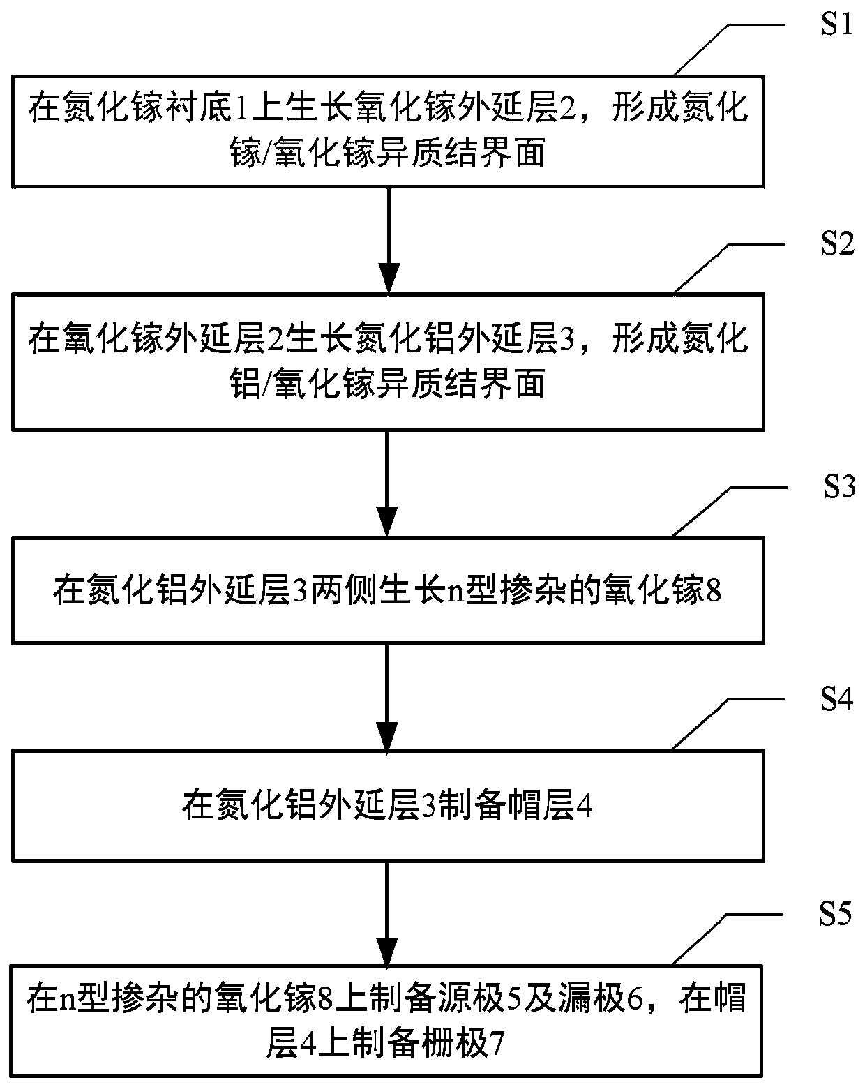
[0037] In order to make the object, technical solution and advantages of the present invention clearer, the present invention will be described in further detail below in conjunction with specific embodiments and with reference to the accompanying drawings.

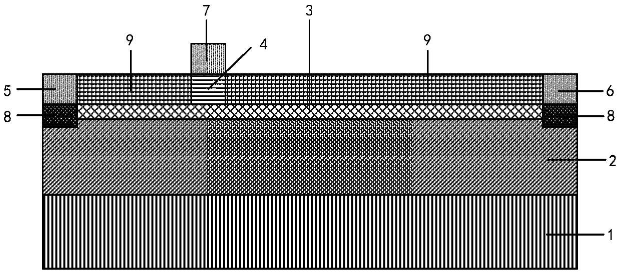
[0038] figure 1 A schematic diagram of a normally-off field effect transistor provided by an embodiment of the present invention is shown. Such as figure 1 As shown, the field effect transistor consists of:

[0039] Gallium Nitride Substrate 1. In the embodiment of the present invention, the gallium nitride substrate 1 has a thickness of 0.1-1 μm, preferably 100 nm, which is not limited in the present invention.

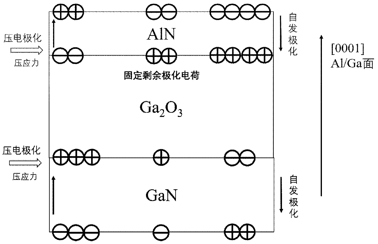
[0040] The gallium oxide epitaxial layer 2 is formed on the gallium nitride substrate 1, and the interface between the gallium nitride substrate 1 and the gallium oxide epitaxial layer 2 forms a gallium nitride / gallium oxide heterojunction interface. In the embodiment of the present invention, the gallium ox...


PUM

PropertyMeasurementUnit
Thicknessaaaaaaaaaa
Thicknessaaaaaaaaaa
Thicknessaaaaaaaaaa

Abstract

The invention discloses a normally-off field effect transistor and a preparation method thereof. The transistor comprises: a gallium nitride substrate (1); a gallium oxide epitaxial layer (2) formed on the gallium nitride substrate (1), wherein a gallium nitride / gallium oxide heterojunction interface is formed at the interface of the gallium oxide epitaxial layer and the gallium nitride substrate;an aluminum nitride epitaxial layer (3) formed on the gallium oxide epitaxial layer (2), wherein an aluminum nitride / gallium oxide heterojunction interface is formed at the interface of the aluminumnitride epitaxial layer and the gallium oxide epitaxial layer; and a cap layer (4) formed on the aluminum nitride epitaxial layer (3). According to the transistor, the material characteristics of III-nitride and gallium oxide are fully utilized, and high-density polarized charges are generated at an aluminum nitride / gallium oxide interface; in the aspect of achieving normally-off operation, p-typegallium nitride is adopted as a gate cap layer, so that the threshold voltage is not influenced by an interface state, the reliability of the field effect transistor is enhanced, the resistivity below a channel is improved, and the drain leakage current and the sub-threshold swing are reduced.

Description

technical field [0001] The invention relates to the field of semiconductor devices, in particular to a normally-off field effect transistor and a preparation method thereof. Background technique [0002] Existing semiconductor normally-off field effect transistors are mainly realized by aluminum gallium nitride / gallium nitride (AlGaN / GaN)-based semiconductor materials. Since both AlGaN and GaN have a polarization effect, the AlGaN / GaN interface will generate polarized positive charges to attract electrons, forming a two-dimensional electron gas (2DEG), and transporting electrons through the 2DEG channel at the interface. [0003] The defects of this kind of transistor are as follows: First, the polarized charge of opposite polarity generated at the interface between AlGaN and GaN materials will reduce the net polarized charge density, resulting in a decrease in 2DEG concentration and conductivity, which limits device performance. Second, AlGaN / GaN-based normally-off field e...

Claims


Application Information

Patent Timeline
03 Dec 2019
Publication
CN110534557A
IPC
H01L29/06; H01L29/24; H01L29/778; H01L21/335
CPC
H01L29/0684; H01L29/24; H01L29/66462; H01L29/7783
Inventors
孙海定; 龙世兵