Insulated-gate bipolar transistor
A bipolar transistor and insulated gate technology, which is applied in the field of power semiconductor devices, can solve problems such as crystal defects, yield reduction, leakage current reliability, etc., and achieve the effect of low turn-on voltage characteristics
- Summary
- Abstract
- Description
- Claims
- Application Information
AI Technical Summary
Problems solved by technology
Method used
Image
Examples
Embodiment 1
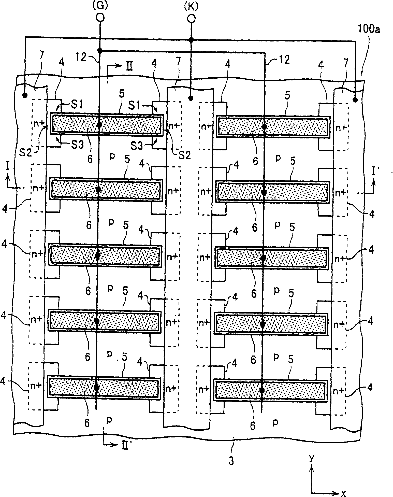
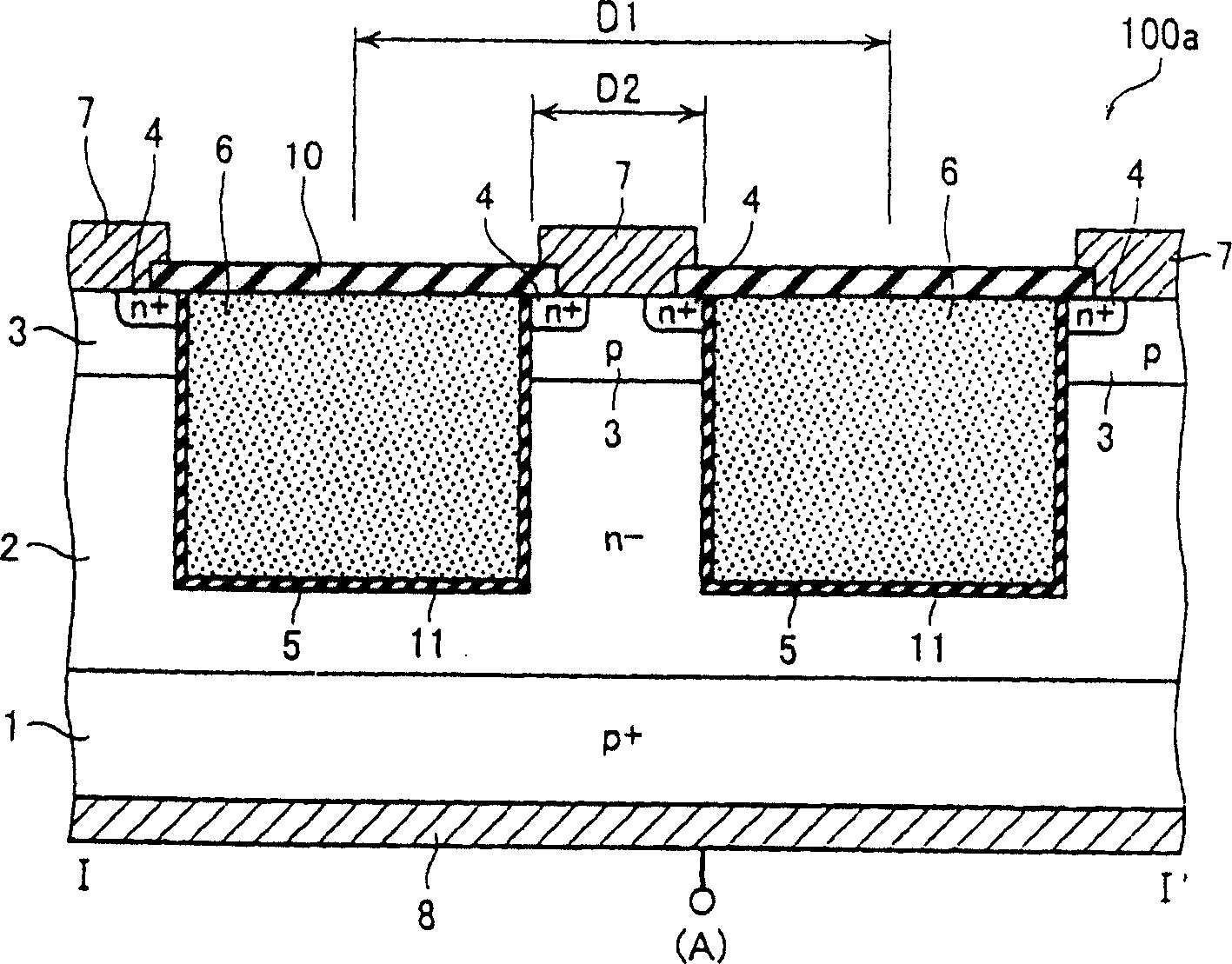
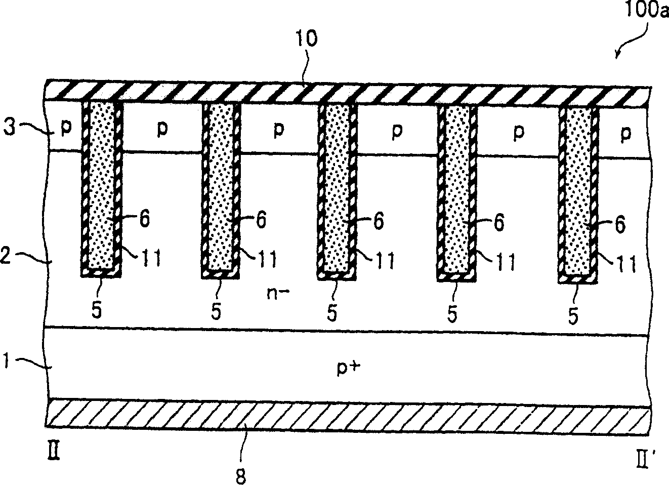
[0037] figure 1 It is a plan view of IGBT100a of an embodiment, figure 2 with image 3 respectively figure 1 I-I' and II-II' sectional views. On the surface of the P-silicon substrate (anode emitter layer) 1, an n-type layer (n-base layer) 2 with a resistivity of 50Ω·cm or more is formed, and a p-base layer 3 with a depth of about 4 μm is formed on the surface . A trench 5 is formed, which penetrates the p base layer 3 to a depth reaching the n base layer 2 , and forms a gate electrode 6 embedded in the trench 5 through the gate insulating film 11 . Hereinafter, the gate electrode 6 is also referred to as an insulating slot gate or simply as a slot gate.
[0038] Such as figure 1 As shown, the insulating trench gate 6 has an elongated rectangular shape on the upper surface, and a plurality of them are arranged at predetermined intervals in the width direction (y direction). The slot grid 6 is also arranged in multiples in its length direction (x direction), for exam...
Embodiment 2
[0050] Image 6 It is a plan view of IGBT100b of Embodiment 2, and its I-I' and II-II' sections are the same as figure 2 and image 3 same. In Embodiment 2, the shape of the cathode emitter layer 4 is different from Embodiment 1. That is, like the cathode electrode 7 , the cathode emitter layer 4 is formed on both ends of the insulating trench gate 6 as an impurity diffusion layer connecting between the plurality of insulating trench gates 6 arranged in the y direction. The situation that the cathode emitter layer 4 is opposite to the three sides of each end of the groove grid is the same as that of the first embodiment.
[0051] According to such a structure, in addition to obtaining the same effect as in Example 1, the accuracy of alignment with the cathode emitter layer 4 can be eased when forming the trench 5, so that the manufacturing margin can be increased.
Embodiment 3
[0053] Figure 7 is a plan view of IGBT100c of Example 3, Figure 8 Is its I-I' profile. II-II' section and image 3 same. In this embodiment, the cathode emitter layer 4 is formed as an impurity diffusion layer continuous between two adjacent insulating trench gates 6 in the x direction, and is shared by the two insulating trench gates 6 . The situation that the cathode emitter layer 4 is opposite to the sides 3 of the respective ends of the groove grid is the same as that of the first embodiment. Cathode emitter layer 4 dispersedly formed in the y direction serves as conduction between cathode electrode 7 and p base layer 3 .
[0054] According to such a structure, in addition to obtaining the same effect as in Example 1, the accuracy of alignment with the cathode emitter layer 4 can be eased when forming the trench 5, so that the manufacturing margin can be increased.
PUM
 Abstract
Description
Claims
Application Information
 - R&D
- Intellectual Property
- Life Sciences
- Materials
- Tech Scout
- Unparalleled Data Quality
- Higher Quality Content
- 60% Fewer Hallucinations
Browse by: Latest US Patents, China's latest patents, Technical Efficacy Thesaurus, Application Domain, Technology Topic, Popular Technical Reports.
© 2025 PatSnap. All rights reserved.Legal|Privacy policy|Modern Slavery Act Transparency Statement|Sitemap|About US| Contact US: help@patsnap.com


