Laminated material and lamination method by using mask with preset pattern on substrate

A technology of layer materials and luminescent material layers, which is applied in the field of color display equipment, can solve problems such as component damage, and achieve the effects of improving precision, reducing costs, and increasing lifespan

Inactive Publication Date: 2006-07-19
SANYO ELECTRIC CO LTD
View PDF0 Cites 0 Cited by
  • Summary
  • Abstract
  • Description
  • Claims
  • Application Information

AI Technical Summary

Problems solved by technology

[0016] However, when the mask is in contact with the substrate, the anode and other components formed on the glass substrate can be damaged by the mask

Method used


Image

  • Laminated material and lamination method by using mask with preset pattern on substrate
  • Laminated material and lamination method by using mask with preset pattern on substrate
  • Laminated material and lamination method by using mask with preset pattern on substrate

Examples


Embodiment Construction

[0048] An organic EL display device produced by the method for producing a color display device according to the present invention will be described below.

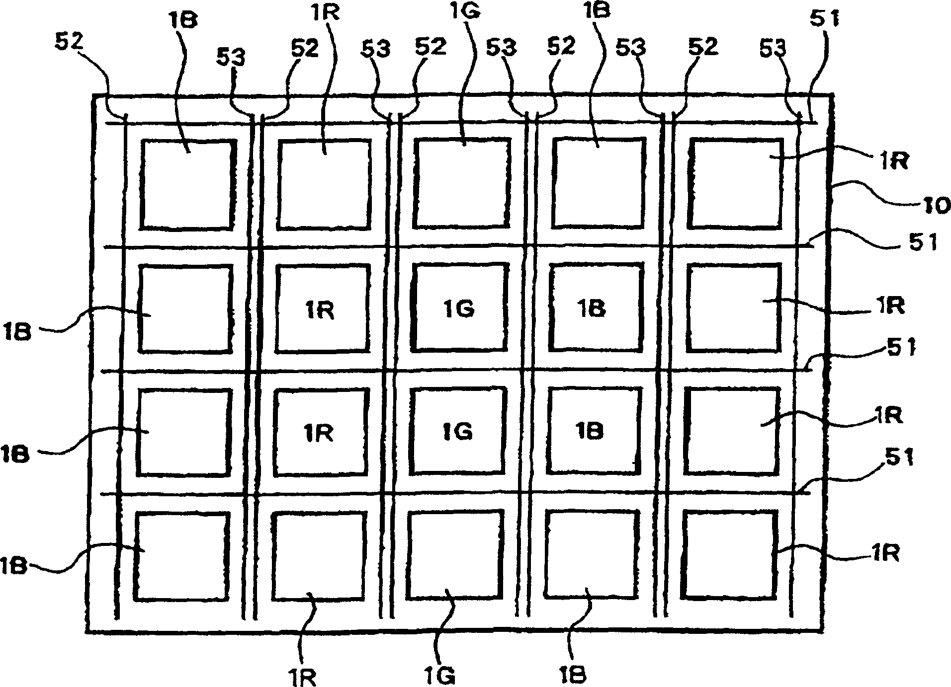
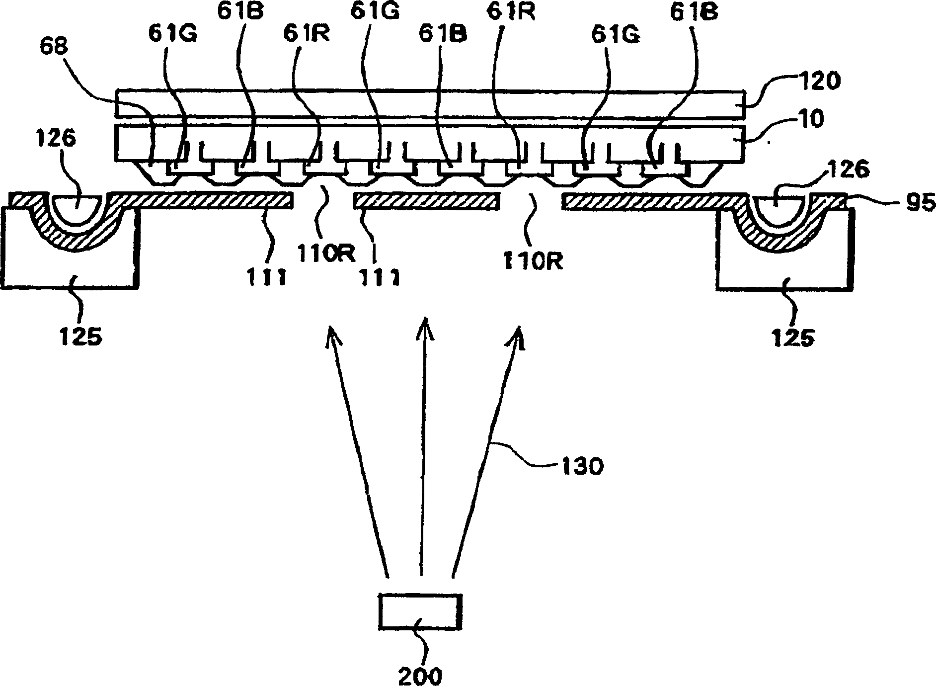
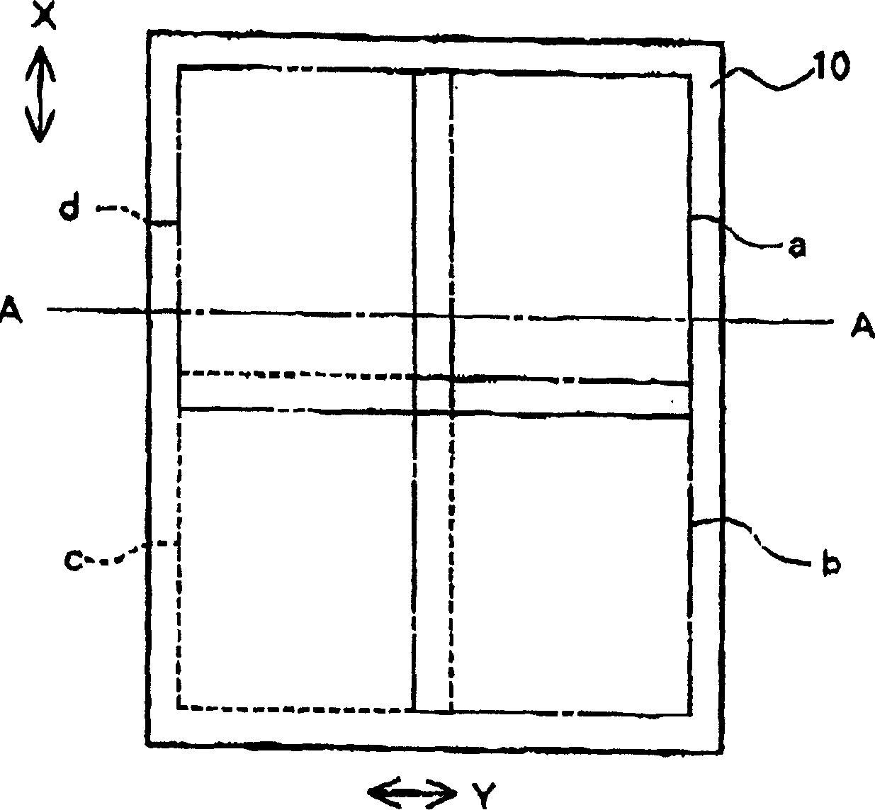
[0049] image 3 A planar structure is shown illustrating a method for moving an insulating substrate onto which an organic material is evaporated according to the inventive method for producing a color display device, and Figure 4 show along image 3 The cross-sectional structure cut by the line A-A in . It should be noted that, Figure 4 Shows a cross section at the step of evaporating organic light-emitting materials of each color onto an insulating substrate such as a glass substrate 10 having a part corresponding to a TFT, an anode of an organic EL element, and a cover for covering by an evaporation method An insulating film 68 surrounding the region of the anode, and in this particular embodiment a red light-emitting element layer, is deposited onto the anode 61R by evaporation.

[0050] The evaporation mask 100...


PUM

PropertyMeasurementUnit
thicknessaaaaaaaaaa

Abstract

Upon formation of a layer such as an emissive layer of an organic EL element by attaching an emissive material onto a substrate (10), an evaporation mask (100) including an opening (110) corresponding to the layer formed to have a plurality of individual patterns and having an area, for example, smaller than the substrate is disposed between the substrate (10) and a material source (200). A relative position between the mask (100) and the material source (200), and the substrate (10) is slid by a predetermined pitch corresponding to the size of a pixel of the substrate (10), thereby forming a material layer (such as the emissive layer 64) in a predetermined region of the substrate. As a result, the material layer can be formed on the substrate through, for example, evaporation with a high accuracy.

Description

technical field [0001] The present invention relates to a color display device using an electroluminescent (hereinafter referred to as "EL") element as a light-emitting element, and a method of manufacturing such a color display device. Background technique [0002] In recent years, EL display devices incorporating EL elements have been considered as potential replacements for CRTs and LCDs. [0003] Active matrix EL display devices (hereinafter referred to as "TFT") including thin film transistors as switching elements for driving EL elements have been developed. [0004] figure 1 Arrangements of display pixels 1R, 1G, and 1B of respective colors in a color organic EL display device are shown. [0005] As shown in the figure, the active matrix organic EL display device includes display pixels 1R, 1G and 1B for red (R), green (G) and blue (B), respectively, which are formed by gate signal lines 51, In the region on the substrate 10 surrounded by the drain signal line 52 a...

Claims


Application Information

Patent Timeline
Patent Type & Authority Patents(China)
IPC IPC(8): H05B33/10H01L33/00C23C14/04G09F9/00G09F9/30H01L27/32H01L51/00H01L51/30H01L51/40H01L51/50H01L51/56H05B33/12
CPCH01L51/0059H01L51/0081H01L51/56H01L27/3211H01L51/0062H01L51/001C23C14/042H01L51/0013H01L51/0011H10K59/35H10K71/18H10K71/164H10K71/166H10K85/649H10K85/631H10K85/324H10K71/00H05B33/10
Inventor 山田努米田清
Owner SANYO ELECTRIC CO LTD
Why Eureka
Try Eureka