Method for integral micromachining multilayer composite structure
A technology of complex structure and seed layer, applied in microstructure technology, microstructure devices, manufacturing microstructure devices, etc., can solve problems such as affecting normal work, increasing the difficulty of precision assembly work, and weak mechanism integrity, and achieves widening processing. range effect
- Summary
- Abstract
- Description
- Claims
- Application Information
AI Technical Summary
Problems solved by technology
Method used
Image
Examples
Embodiment
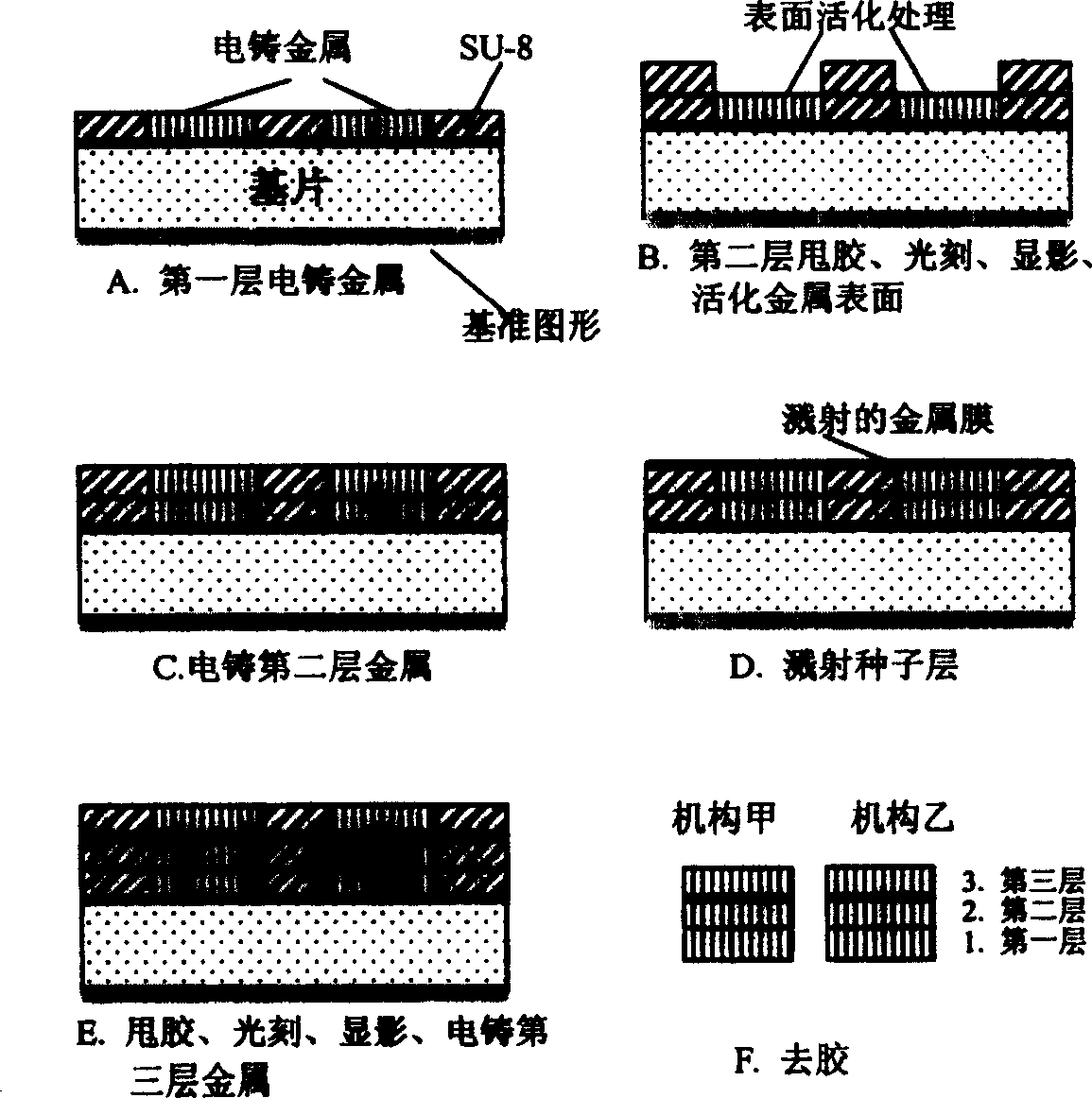
[0016] Process two three-layer structures that are used in conjunction with each other. In this structure, the first and third layers of graphics are larger than the second layer of graphics. The electroforming material is Ni, and a double-sided exposure lithography machine is used. The specific processing method is as follows:
[0017] A photolithography reference pattern is first made on the bottom surface of the substrate, and subsequent photolithography processes are all based on it.
[0018] Such as figure 1 As shown in middle A, the first layer of photoresist SU-8, after photolithography and development according to the reference pattern on the bottom surface, Ni is electroformed, and the surface of the electroformed layer is planarized after electroforming.
[0019] Such as figure 1 As shown in middle B, after the second layer of glue removal, photolithography (based on the bottom surface pattern), and development, the surface of Ni is subjected to surface activation t...
PUM
 Abstract
Description
Claims
Application Information
