Supercharge Your Innovation With Domain-Expert AI Agents!

Layout of static RAM units and device

A technology of active region and gate electrode, applied in semiconductor/solid-state device manufacturing, electrical components, electric solid-state devices, etc.

Inactive Publication Date: 2007-02-28
SAMSUNG ELECTRONICS CO LTD
View PDF3 Cites 0 Cited by
  • Summary
  • Abstract
  • Description
  • Claims
  • Application Information

AI Technical Summary

Problems solved by technology

However, traditionally, full CMOS SRAM cells generally occupy a larger area than corresponding load resistor cells or thin film transistor (TFT) cells

Method used


Image

  • Layout of static RAM units and device
  • Layout of static RAM units and device
  • Layout of static RAM units and device

Examples


Embodiment Construction

[0040] The present invention will be described more fully hereinafter with reference to the accompanying drawings, in which preferred embodiments of the invention are shown. However, the invention may be embodied in different forms and should not be construed as limited to the embodiments described herein. Rather, these embodiments are provided so that this disclosure will be thorough, complete, and will fully convey the scope of the invention to those skilled in the art. In the drawings, the thicknesses of layers and regions are exaggerated for clarity. It will also be understood that when a layer is referred to as being "on" another layer or substrate, it can be directly on the other layer or substrate, or intervening layers may also be present. Like reference numerals designate like elements throughout.

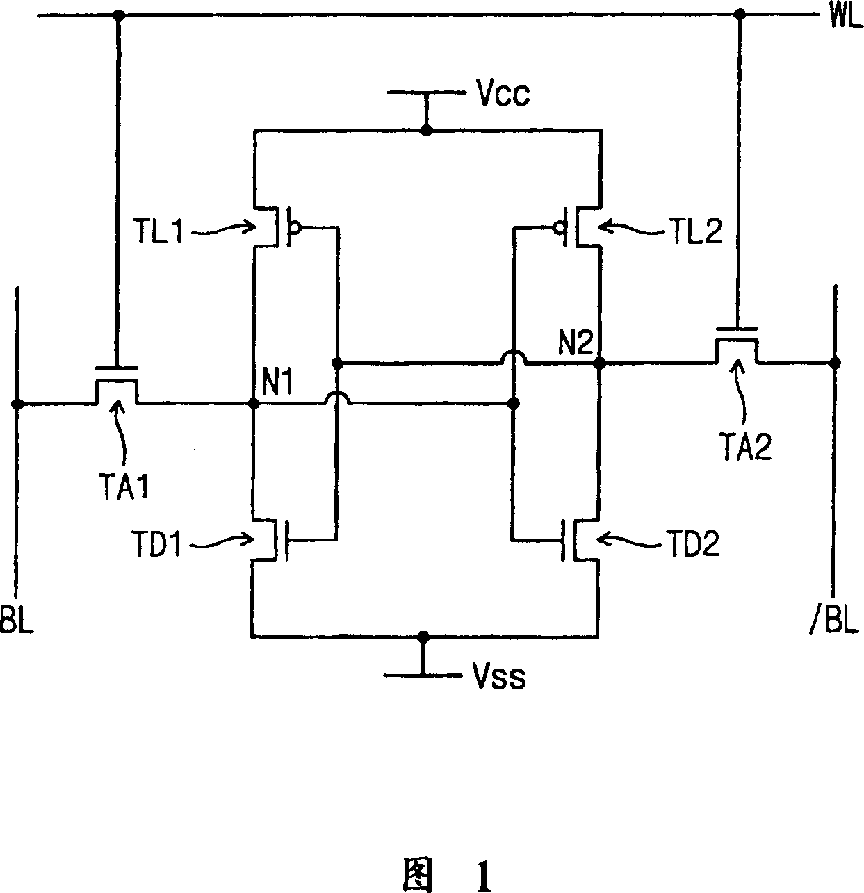
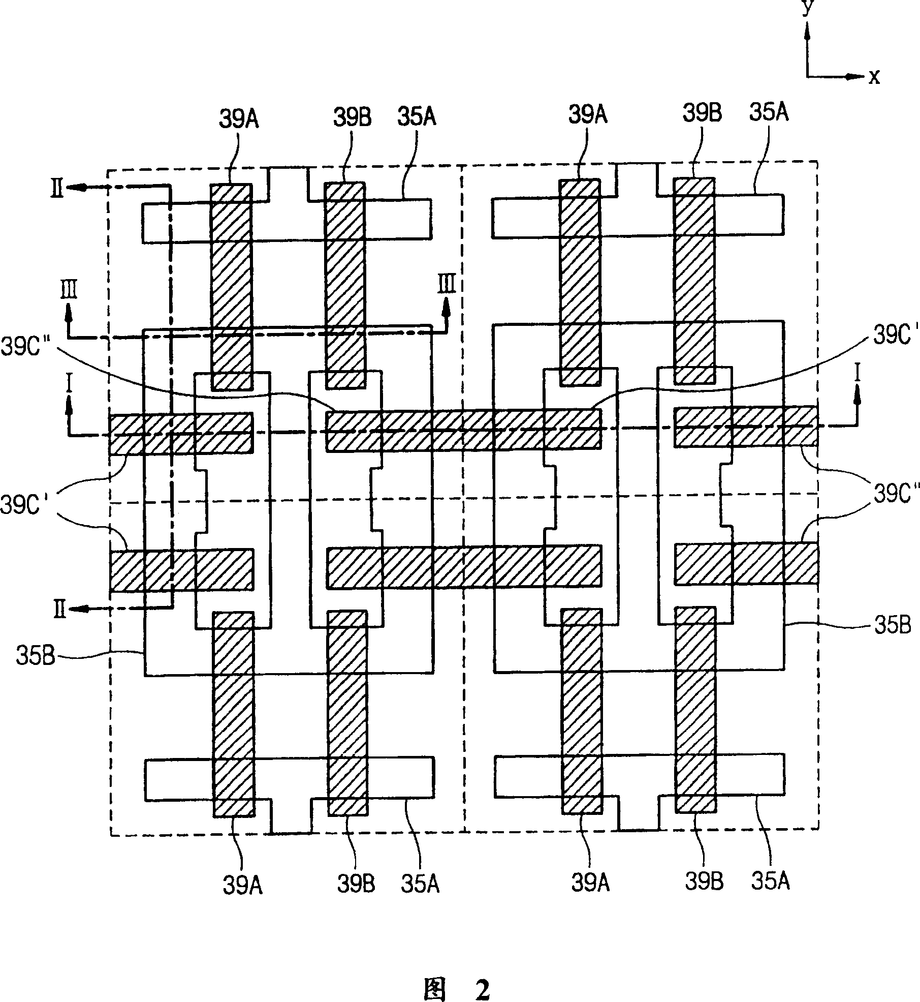
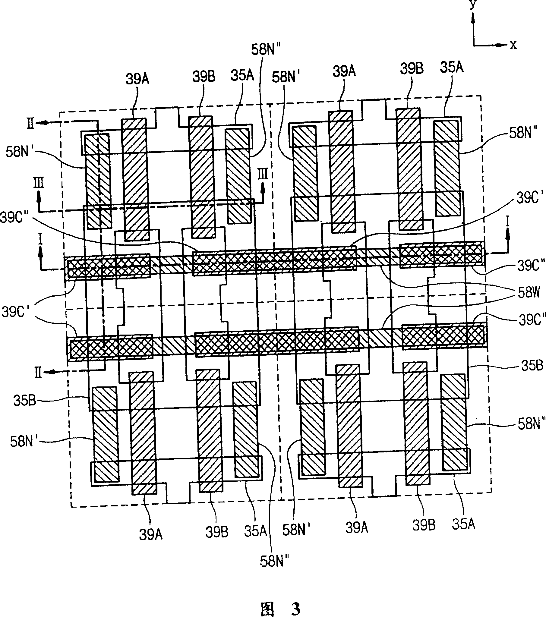
[0041] 2 to 6 are top views illustrating full CMOS SRAM cells according to embodiments of the present invention. Four units are shown in each figure, however, additiona...


PUM


Abstract

SRAM cells and devices are provided. The SRAM cells may share connections with neighboring cells, including ground, power supply voltage and / or bit line connections. SRAM cells and devices are also provided that include first and second active regions disposed at a semiconductor substrate. Parallel first and second gate electrodes cross over the first and second active regions. One end of the first active region adjacent to the first gate electrode is electrically connected to the second active region adjacent to the first gate electrode through a first node line parallel to the first gate electrode, and the other end of the first active region adjacent to the second gate electrode is electrically connected to the second active region adjacent to the second gate electrode through a second node line parallel to the second gate electrode. The first node line is electrically connected to the second gate electrode through a first local interconnection crossing over the first node line, and the second node line is electrically connected to the first gate electrode through a second local interconnection crossing over the second node line. Additionally, a word line may be in direct contact with gate electrodes of transfer transistors of the SRAM cells.

Description

technical field [0001] The present invention relates to a semiconductor device, and more particularly, to a complementary metal oxide semiconductor (CMOS) static random access memory (SRAM) cell. Background technique [0002] Memory devices are widely used in electronic devices to store data. Typically, such memory devices can be divided into at least two categories: dynamic random access memory (DRAM) and static random access memory (SRAM). DRAM generally refreshes the data periodically by rewriting data into the memory to keep the data. In contrast, SRAM generally does not require this refresh. For example, SRAM devices are widely used in cache memory in computers and portable equipment. [0003] Generally, memory cells of an SRAM device can be divided into two categories. One type of memory cell includes a load resistor as a load device of the memory cell. The other type is a CMOS type unit that uses a transistor as the load device of the memory unit. [0004] Memor...

Claims


Application Information

Patent Timeline
Patent Type & Authority Patents(China)
IPC IPC(8): H01L27/11H10B10/00
CPCH01L27/1104H01L27/11H10B10/00H10B10/12H10B99/00
Inventor 金成奉郑舜文朴宰均
Owner SAMSUNG ELECTRONICS CO LTD
Features
  • R&D
  • Intellectual Property
  • Life Sciences
  • Materials
  • Tech Scout
  • Unparalleled Data Quality
  • Higher Quality Content
  • 60% Fewer Hallucinations
Learn More