
Liquid crystal display device built-in finger printing device and method of manufacturing the same

一种液晶显示装置、指纹的技术,应用在静态指示器、字符和模式识别、获取/整理指纹/掌纹等方向,能够解决制造过程管理困难、图像质量下降、少设计余量等问题,达到提高图像显示质量、容易管理、增加设计余量的效果

Inactive Publication Date: 2007-06-06
SAMSUNG ELECTRONICS CO LTD
View PDF1 Cites 2 Cited by
  • Summary
  • Abstract
  • Description
  • Claims
  • Application Information

AI Technical Summary

Problems solved by technology

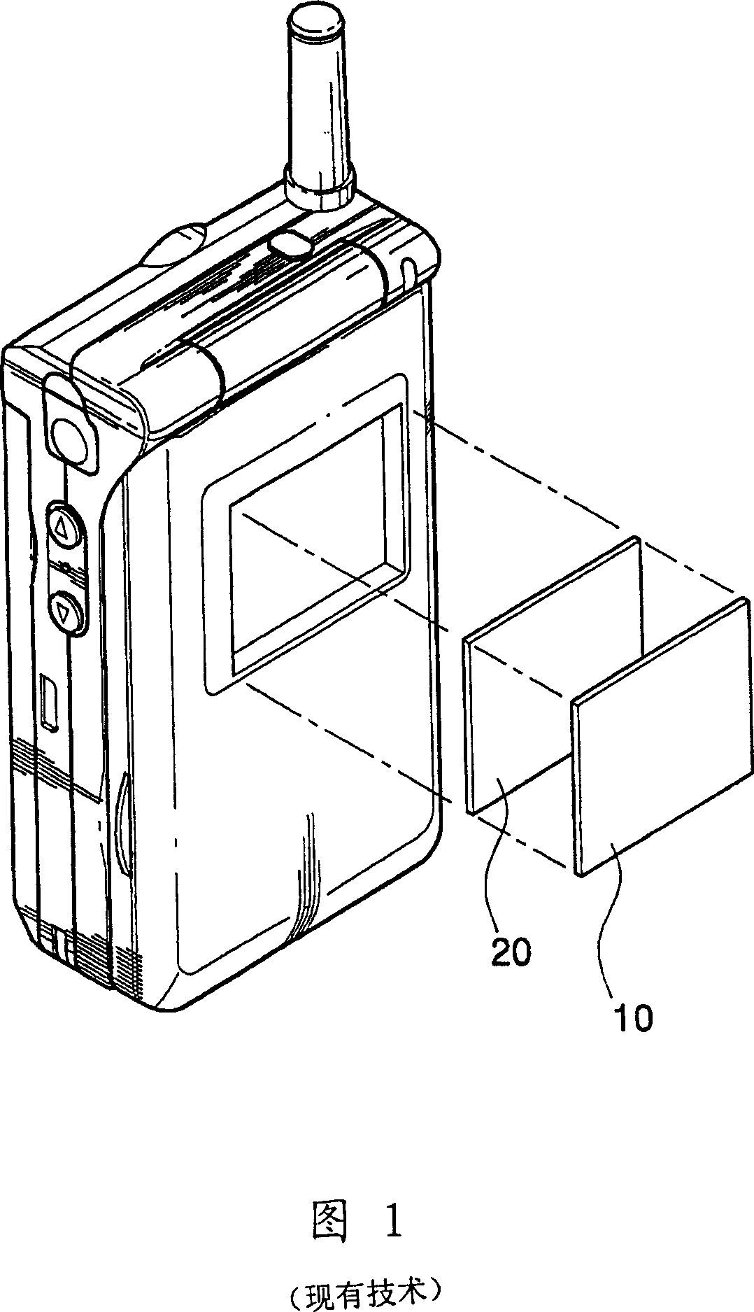
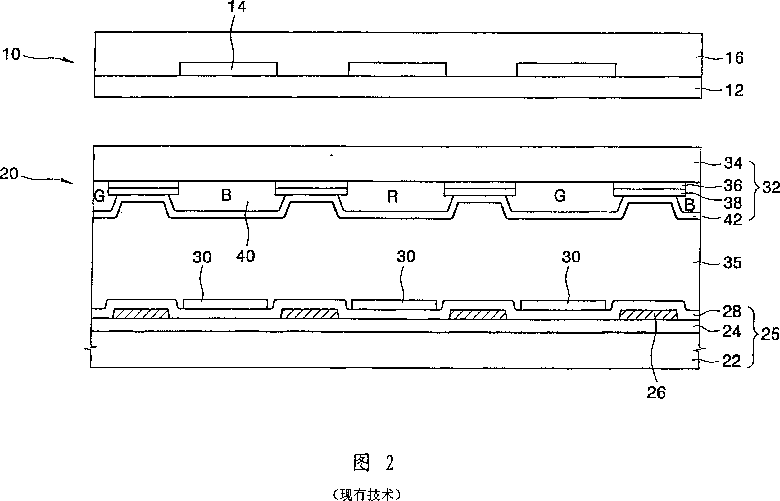
When the TFT fingerprint recognition substrate 10 is not precisely aligned with the TFT-LCD panel 20, the aperture ratio (aperture ratio) of the TFT fingerprint recognition substrate 10 may be reduced by n times compared with the aperture ratio of the TFT-LCD panel 20
[0016] In particular, when the TFT substrate 25 of the TFT-LCD panel 20 is not precisely aligned with the color filter substrate 32 of the TFT-LCD panel 20, the aperture ratio is greatly reduced.
Therefore, little design margin may be left and management of the manufacturing process may be difficult
[0017] In addition, the precise alignment process may not be easy to complete, and when designing the TFT-LCD panel 20 mounted with the TFT fingerprint identification substrate 10 considering the misalignment between the substrates, the image quality may be degraded due to the reduced aperture ratio

Method used


Image

  • Liquid crystal display device built-in finger printing device and method of manufacturing the same
  • Liquid crystal display device built-in finger printing device and method of manufacturing the same
  • Liquid crystal display device built-in finger printing device and method of manufacturing the same

Examples


Embodiment Construction

[0044] Hereinafter, preferred embodiments of the present invention will be described in detail with reference to the accompanying drawings.

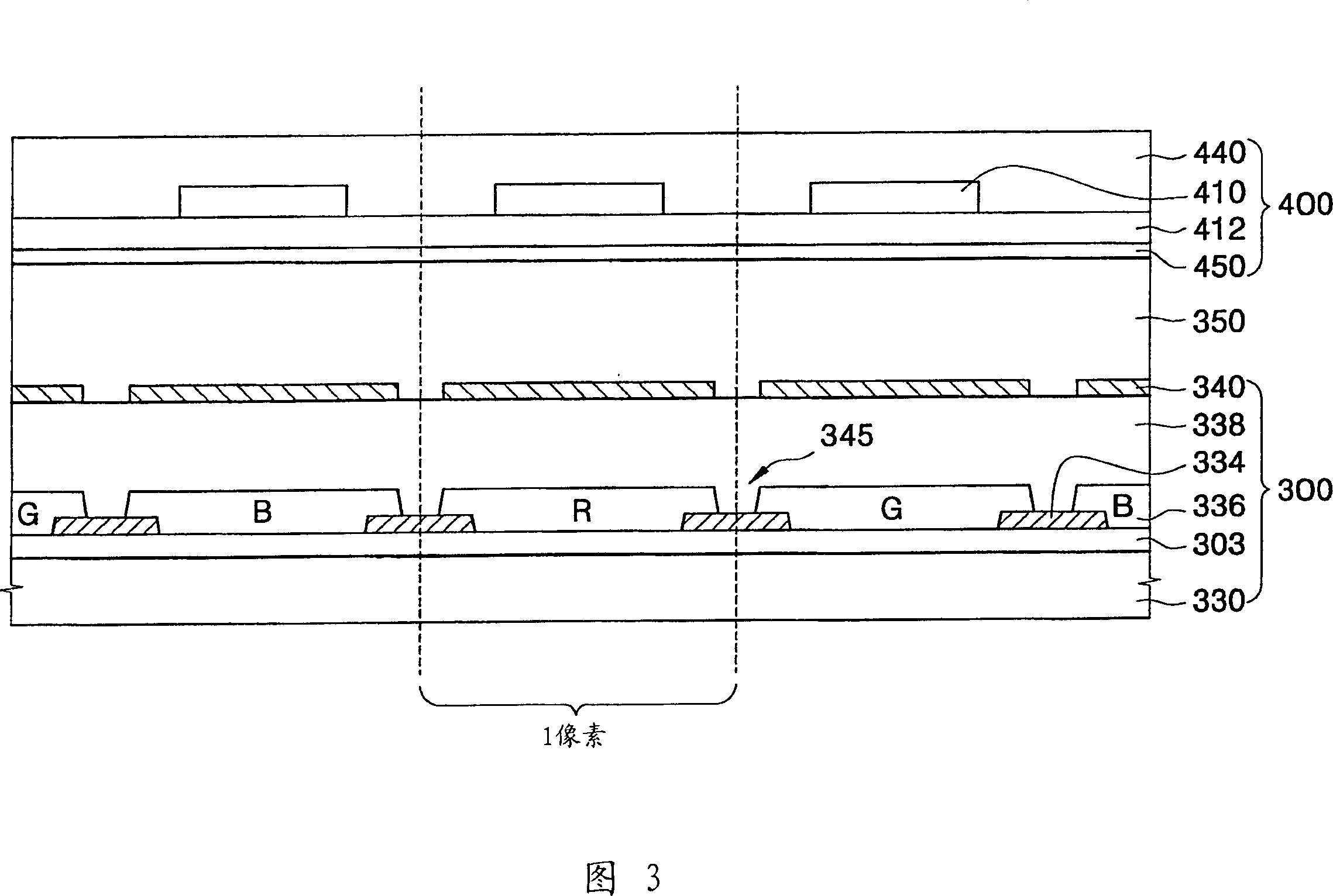
[0045] 3 is a cross-sectional view showing a color filter structure on an array of an α-Si TFT-LCD panel mounted with a TFT fingerprint recognition substrate according to an exemplary embodiment of the present invention.

[0046] The on-array color filter structure refers to a structure in which a color filter is formed on a TFT substrate to align it with the thin film transistor of the TFT substrate. That is, the color filter and the thin film transistor have a self-aligned structure. Therefore, the aperture ratio of the TFT-LCD panel is improved. In addition, the color filter can be precisely aligned with the thin film transistors of the TFT substrate.

[0047] Referring to FIG. 3, a TFT fingerprint recognition substrate 400 is attached to a TFT-LCD panel having a color filter structure on an array.

[0048] The TFT fingerprint recognition...


PUM


Abstract

A liquid crystal display device having fingerprint identification device for enhancing aperture ratio and transmissivity of a TFT-LCD panel is disclosed. A fingerprint identification substrate (400) is attached to a TFT substrate (300). The TFT substrate has color-filter-on-array structure in which the color filters (336) and the thin film transistors can be eliminated, the aperture ratio is increased, and the quality of image display is enhanced. In addition, the transmissivity is increased according to the decrease of the number of glass substrate used in the liquid crystal display device, so that the sensitivity of fingerprint identification is enhanced.

Description

Technical field [0001] The present disclosure relates to a liquid crystal display device with a built-in fingerprint identification device and a method of manufacturing the liquid crystal display device. Background technique [0002] Amorphous silicon (α-Si) thin film transistor liquid crystal display device (TFT-LCD) is a type of flat panel display (FPD). α-Si TFT-LCD devices are used in laptop computers, monitors, televisions, and mobile phones. [0003] The α-Si TFT-LCD device displays images by switching thin film transistors. In addition, α-SiTFT-LCD devices also have photosensitive characteristics and are used as optical sensors in the field of biostatistics. [0004] In personal verification systems, fingerprint identification methods using fingerprint identification devices are particularly widely used, because fingerprint identification methods can be implemented at a very low cost and have the characteristics of high usability and high accuracy. [0005] Conventional fi...

Claims


Application Information

Patent Timeline
Patent Type & Authority Patents(China)
IPC IPC(8): G06K9/00G02F1/133G02F1/13G02F1/1368
CPCG06K9/0004G02F2001/13312G02F1/13338G02F1/13312G06V40/1318G02F1/13
Inventor 宋溱镐梁成勋蔡钟哲崔埈厚
Owner SAMSUNG ELECTRONICS CO LTD
Learn More