

Electrostatic discharge preventing method for display and electrostatic discharge preventing device
An electrostatic discharge protection and electrostatic discharge technology, which is applied in electrostatic, instruments, circuits, etc., can solve the problems of inefficiency of layout area, easy to cause damage, and failure of electrostatic discharge protection circuit.
- Summary
- Abstract
- Description
- Claims
- Application Information
AI Technical Summary
Problems solved by technology
Method used
Image

Examples
Embodiment Construction
[0029] In order to make the above-mentioned and other purposes, features, and advantages of the present invention more clearly understood, the preferred embodiments are specifically listed below, together with the accompanying drawings, and are described in detail as follows:
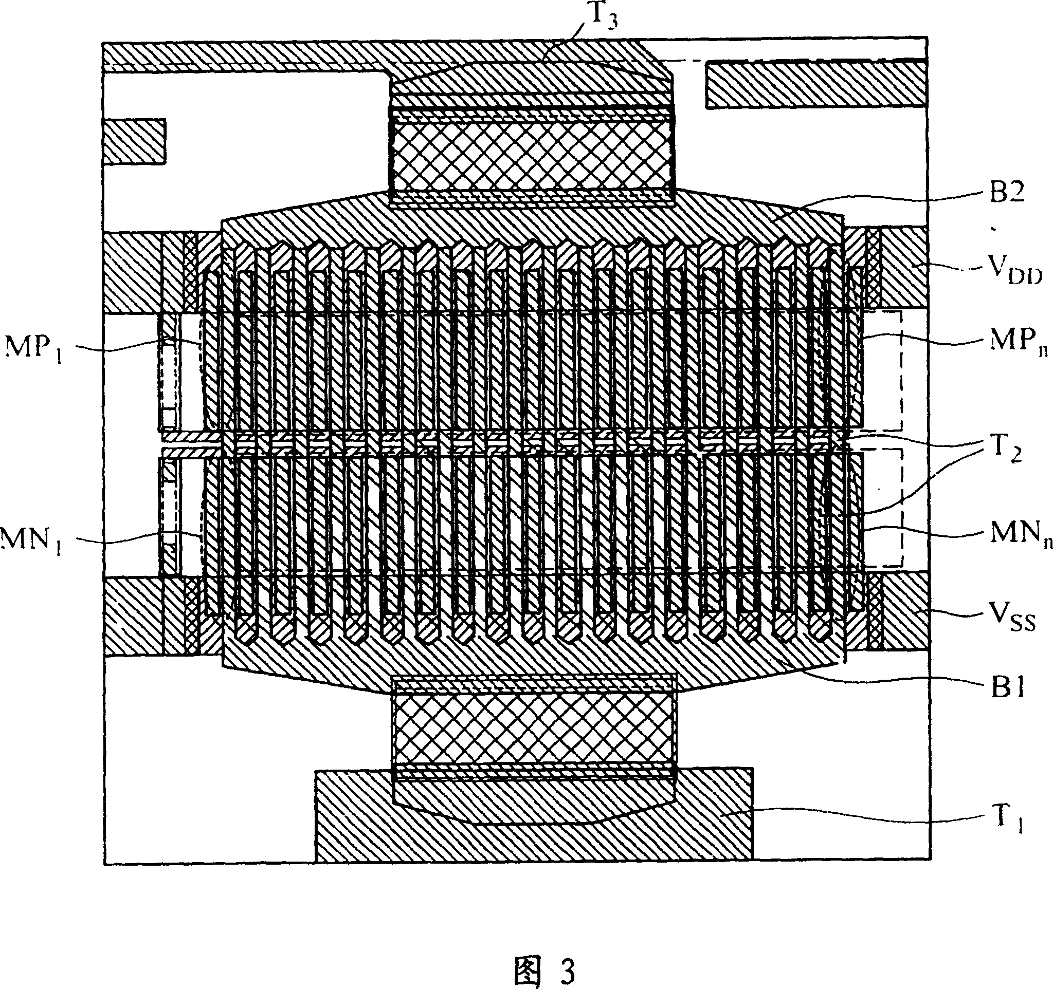
[0030] FIG. 3 shows a layout of an ESD protection circuit manufactured according to the ESD protection method of the present invention.
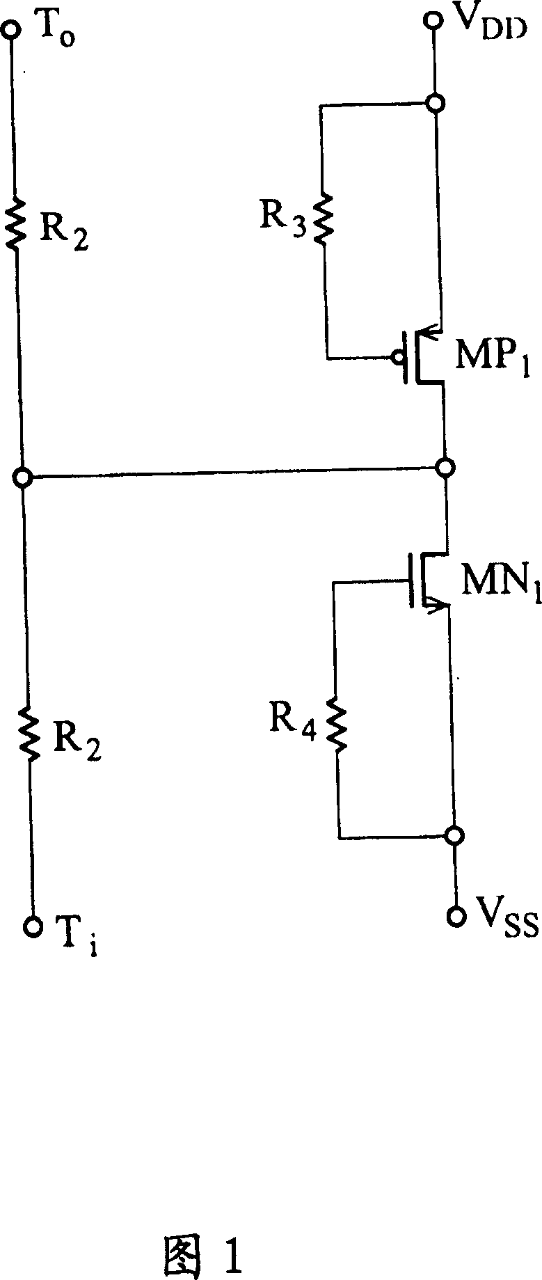
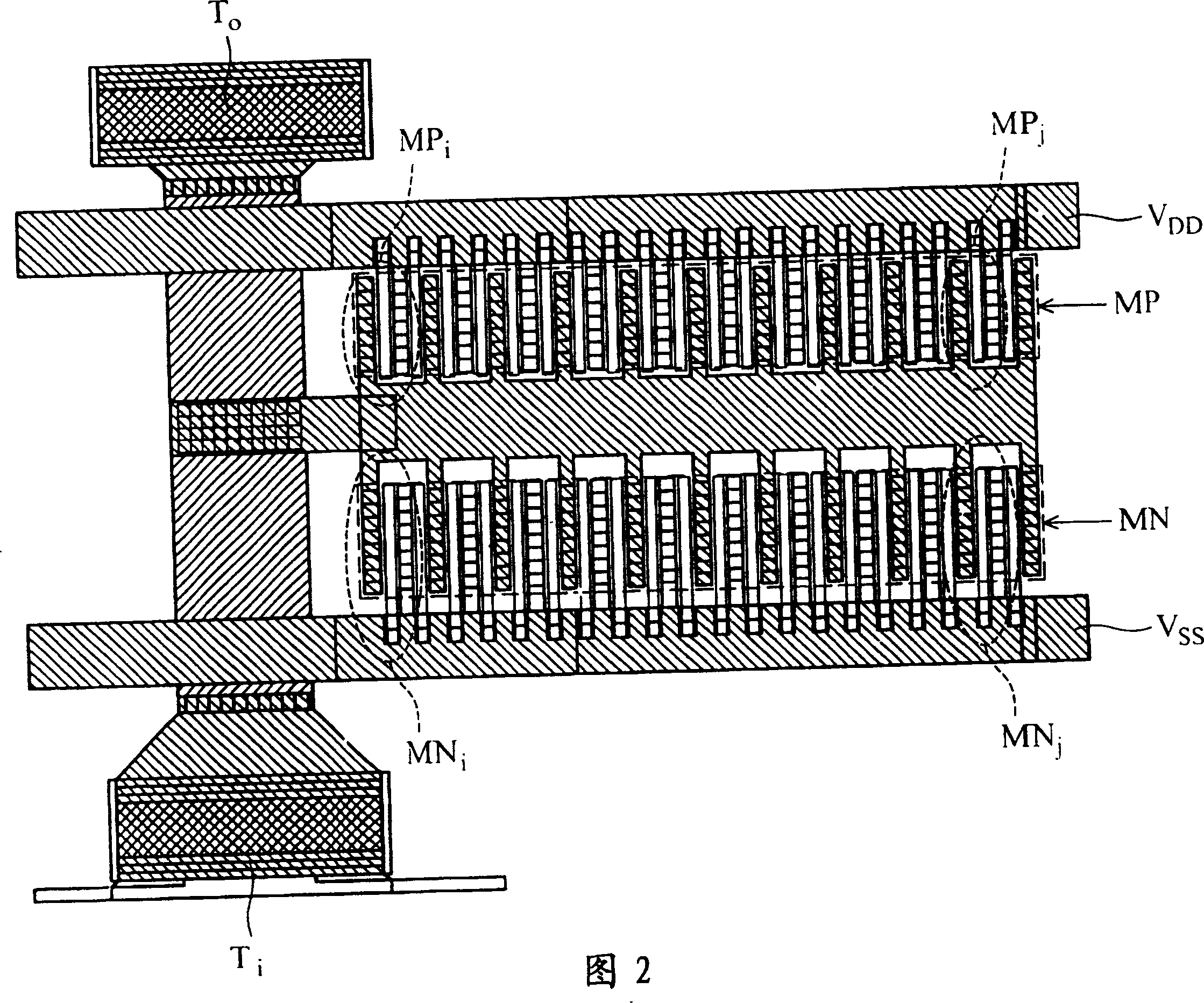
[0031] Various ESD protection units (or components) in the present invention can be manufactured before or after forming the input signal lines. In this embodiment, it is fabricated after the input signal line is fabricated, and the electrostatic discharge protection unit (MP 1 ~MP n and MN 1 ~MN n ) are composed of PMOS transistors and NMOS transistors respectively. Through a specific connection method (the connection method shown by the MOS transistor in Figure 1), the above-mentioned electrostatic protection unit (MP 1 ~MP n and MN 1 ~MN n ) can have a func...
PUM
 Abstract
Description
Claims
Application Information