Plasma displaying board using spiral-wave plasma source
A plasma and display panel technology, applied to AC plasma display panels, solid cathode parts, instruments, etc., can solve the problem of low plasma density and achieve the effect of increasing plasma density
- Summary
- Abstract
- Description
- Claims
- Application Information
AI Technical Summary
Problems solved by technology
Method used
Image

Examples
Embodiment Construction
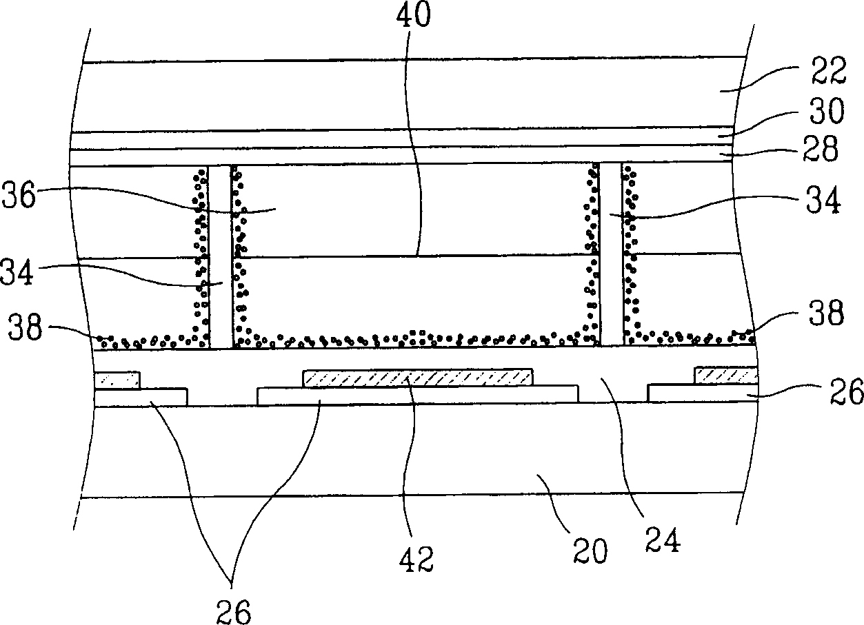
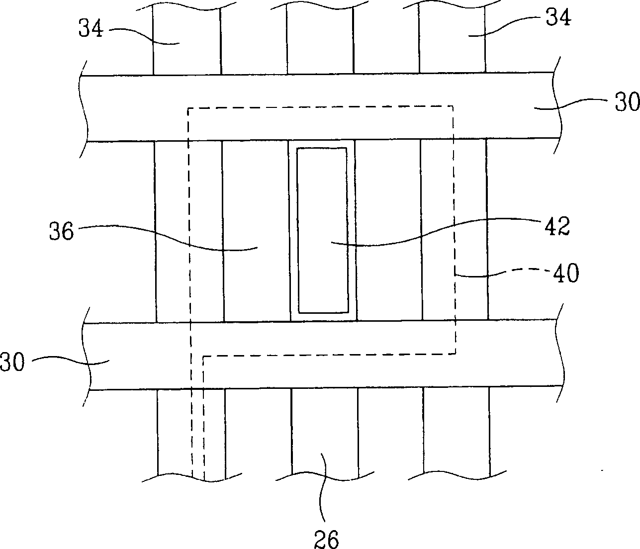
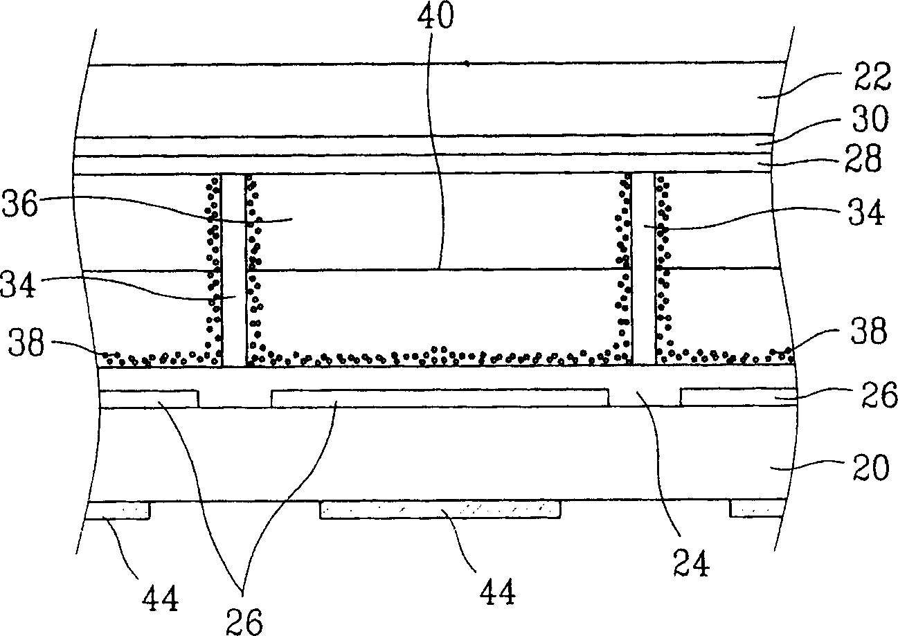
[0024] figure 1 is a partial sectional view of a plasma display panel (PDP) according to a first embodiment of the present invention. As shown in the figure, a first substrate 20 and a second substrate 22 define the exterior of the PDP, the two substrates being arranged substantially in parallel with a predetermined gap therebetween.
[0025] On the surface of the first substrate 20 opposite to the second substrate 22 are formed a plurality of address electrodes 26 arranged in parallel in stripes and a transparent insulating layer 24 covering the address electrodes 26 . On the surface of the second substrate 22 opposite to the first substrate 20, a plurality of discharge sustain electrodes 30 arranged in parallel in stripes are formed and are perpendicular to the address electrodes 26 formed on the first substrate 20, covering the discharge sustain electrodes. The transparent insulating layer 28 of the electrode 30, and a transparent protective layer (not shown) made of a ma...
PUM
 Abstract
Description
Claims
Application Information
 - R&D
- Intellectual Property
- Life Sciences
- Materials
- Tech Scout
- Unparalleled Data Quality
- Higher Quality Content
- 60% Fewer Hallucinations
Browse by: Latest US Patents, China's latest patents, Technical Efficacy Thesaurus, Application Domain, Technology Topic, Popular Technical Reports.
© 2025 PatSnap. All rights reserved.Legal|Privacy policy|Modern Slavery Act Transparency Statement|Sitemap|About US| Contact US: help@patsnap.com