Substrate binding device and method

A technology for bonding devices and substrates, applied in non-electric welding equipment, instruments, static indicators, etc., can solve problems such as inability to remove dust and dust, reduce yield, disturb airflow, etc., to suppress dust and dust flying, and ease sharp The effect of vacuuming

Inactive Publication Date: 2003-09-03
SHIBAURA MECHATRONICS CORP
View PDF0 Cites 6 Cited by
  • Summary
  • Abstract
  • Description
  • Claims
  • Application Information

AI Technical Summary

Problems solved by technology

[0020] Although the cleanliness of the manufacturing site is as high as possible, it is practically impossible to make the dust and dust contained in the air completely zero, and since the substrate bonding device includes mechanically movable parts, from the mechanism Partial generation of new dust, etc. is inevitable, so it is often impossible to remove such dust and dust trapped in the chamber
[0021] Moreover, when the substrates are bonded, when the vacuum pump is started to evacuate the chamber 2, the rapid exhaust action at the start of the vacuum pump operation will disturb the airflow in the chamber 2, so that dust and dust trapped in the lower chamber 2b will fly. , the risk of being attached to the display surface of the substrate 1b
[0022] Moreover, the adhesion of dust and dust on the substrate after bonding also tends to degrade the electrical characteristics of the substrate
When the vacuum after bonding in the chamber 2 is broken, the airflow for restoring the air pressure will also cause dust and dust in the chamber 2 to fly, adhere to the electrode surface, and damage the electrical conduction with the connected IC, etc.
[0023] Moreover, the requirements for the display screen are becoming more and more refined nowadays, even if there is extremely small dust and dust in the chamber, it will fly up due to the airflow generated when the vacuum is vacuumed or broken, and it will adhere to the display surface and the electrode part, reducing the manufacturing cost. Yield, and thus want to improve

Method used


Image

  • Substrate binding device and method
  • Substrate binding device and method
  • Substrate binding device and method

Examples


Embodiment approach

[0062] Refer to the following Figure 3 to Figure 13 , the embodiment of the substrate bonding device and the substrate bonding method according to the present invention will be described in detail. In these figures, with figure 1 with figure 2 The structures that are the same as the existing structures shown are assigned the same symbols, and detailed description thereof will be omitted.

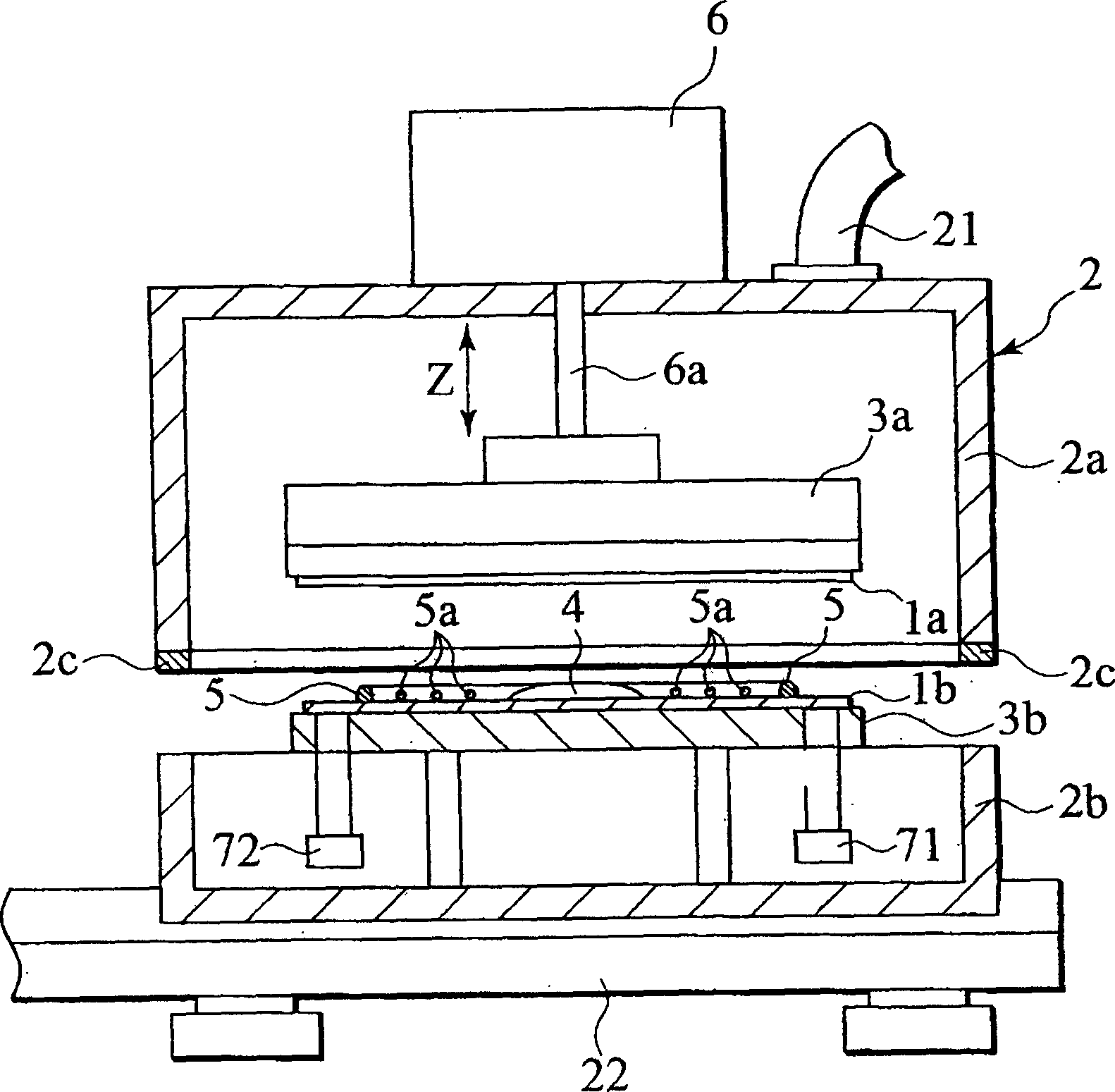
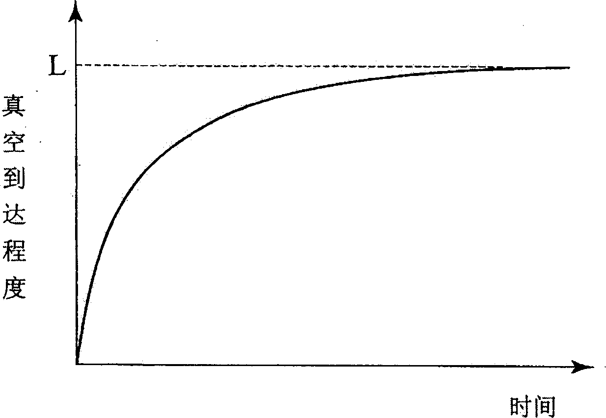
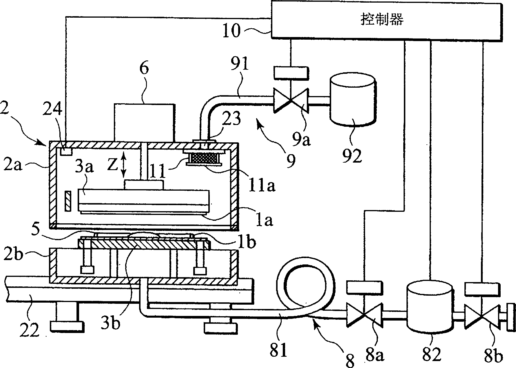
[0063] image 3 It is a sectional view showing the main part of the first embodiment of the substrate bonding device of the present invention used in the manufacture of drop-type liquid crystal display panels; Figure 4 yes means image 3 In the shown device, when the valve is controlled by the controller, the characteristic curve of the attainment degree of the vacuum degree in the chamber changes.

[0064] Such as image 3 As shown, a pair of upper and lower rectangular peeling substrates 1a, 1b are held on the bottom of the upper chuck 3a and the upper surface of the lower chuck 3...


PUM


Abstract

The present invention relates to an improved excellent substrate laminating apparatus and method, which are good for manufacturing liquid crystal display panel. For the vacuum pumping performing of a chamber (2), the opening of a valve (8a) communicating with a vacuum pump (82) is controlled to change the intake resistance of a pipe (81) from high to low, and to suppress an exhaust air stream occurring when vacuum pumping is started. Furthermore, in the process (vacuum venting) for recovering the atmosphere pressure in the chamber (2), a recovery valve (9a) is controlled to change from high to low, the inflow resistance of a gas introduced into the chamber (2), so that the amount of the gas introduced into the chamber (2) at the beginning of the vacuum venting is reduced. Therefore, since the air stream in the chamber (2) can be moderated during the vacuum pumping and the vacuum venting, the stirring up of dust in the chamber (2) and the attachment of the dust to the substrates can be avoided, and high-quality laminated substrates can be provided at a high manufacturing yield.

Description

technical field [0001] The present invention relates to the improvement of an excellent substrate bonding device and substrate bonding method suitable for manufacturing liquid crystal display panels and the like. Background technique [0002] Liquid crystal display panels used in displays such as personal computers, TV receivers, and various monitors are generally produced by bonding a pair of opposing glass substrates together with an adhesive applied around the display surface. [0003] A liquid crystal display panel is formed by encapsulating liquid crystals in the display surface between two bonded substrates. There are two types of liquid crystal injection and liquid crystal drop in liquid crystal encapsulation in the display surface. Regardless of the encapsulation method of liquid crystals, a plurality of spacers are scattered or even installed on any one of the substrates, and bonding is carried out after maintaining a constant interval (cell gap) between substrates ...

Claims


Application Information

Patent Timeline
Patent Type & Authority Applications(China)
IPC IPC(8): G02F1/13G02F1/133G02F1/1333G02F1/1339
CPCB23K20/02G02F1/133308
Inventor 石山英一
Owner SHIBAURA MECHATRONICS CORP
Why Eureka
Try Eureka