
Mfg. method of semiconductor device with opening portion
A manufacturing method and semiconductor technology, which can be used in semiconductor/solid-state device manufacturing, electrical components, circuits, etc., to solve problems such as metal filling for wiring, disconnection of anti-diffusion films, and reduction in reliability of semiconductor devices.
- Summary
- Abstract
- Description
- Claims
- Application Information
AI Technical Summary
Problems solved by technology
Method used
Image

Examples
Embodiment Construction
[0032] Next, description will be given based on attached drawings of embodiments of the present invention.
[0033] Implementation form 1
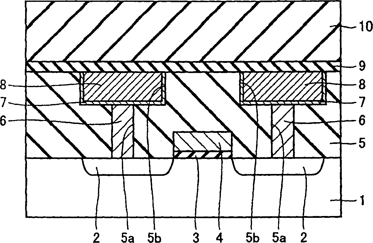
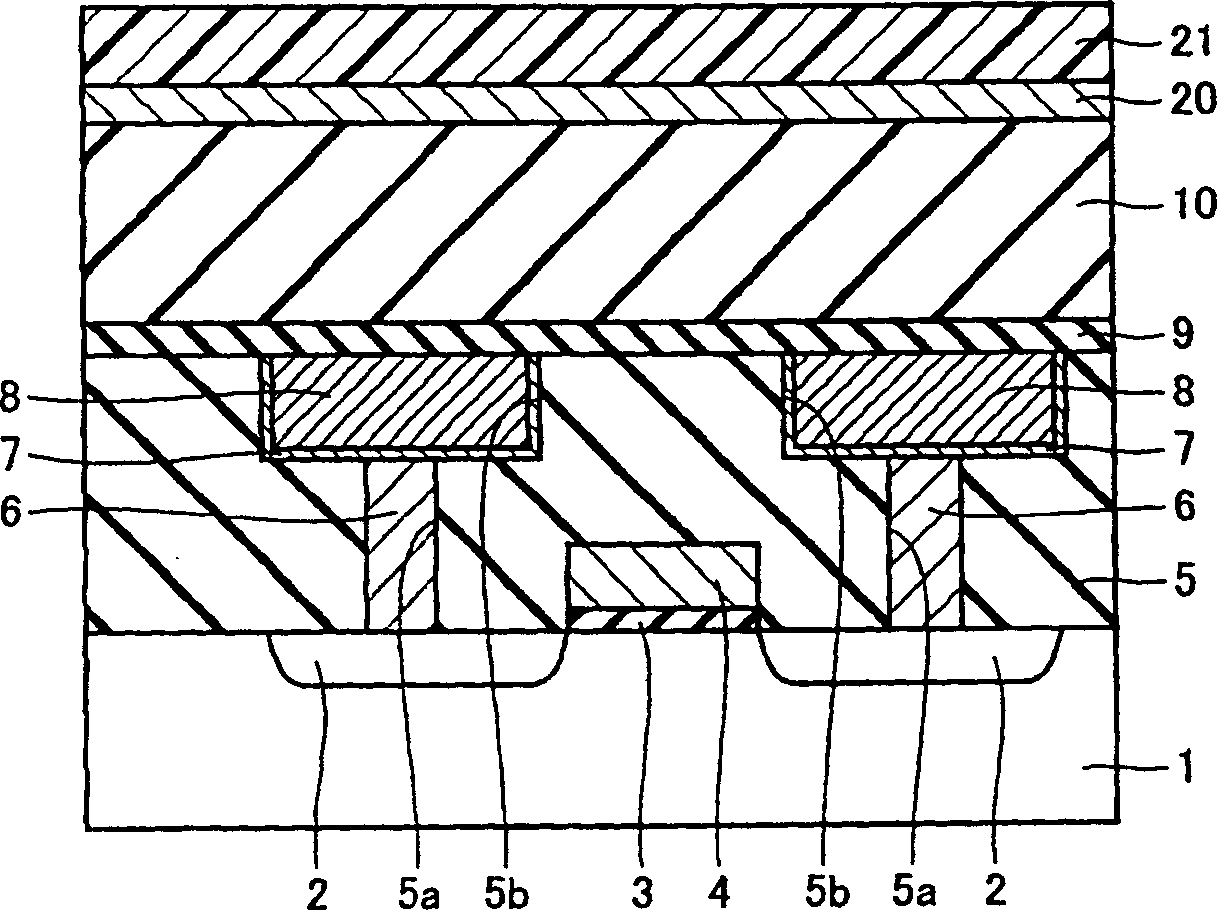
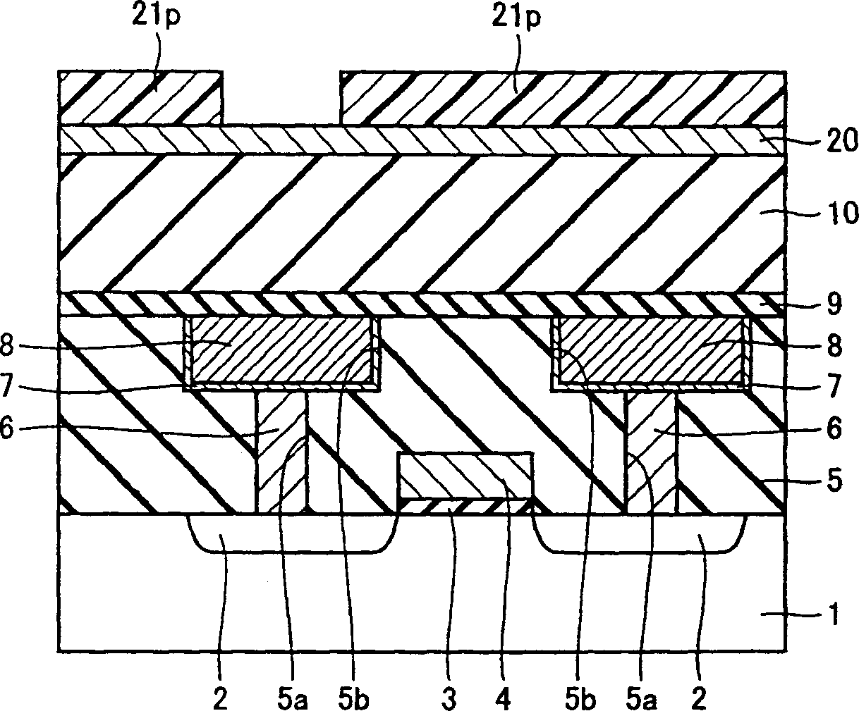
[0034] refer to Figure 1 to Figure 11 , the method of manufacturing the semiconductor device according to the first embodiment will be described. First, if figure 1 As shown, on the surface of the semiconductor substrate 1, MOS transistors and wiring structures connected to the MOS transistors are formed. This MOS transistor includes a pair of source / drain regions 2 formed at a predetermined interval interposed in a channel region, and a gate electrode 4 formed through a gate insulating film 3 on the channel region. In addition, the wiring structure connected to the MOS transistor includes a tungsten plug 6 filled in the via hole 5a formed in the interlayer insulating film 5, and a nitrogen plug formed along the surface of the wiring trench 5b of the interlayer insulating film 5. An anti-diffusion film 7 made of a tantalum oxide (TaN...
PUM
 Abstract
Description
Claims
Application Information