Case for packaging optical device and making method thereof

A technology of optical devices and manufacturing methods, applied in laser parts, lasers, semiconductor lasers, etc., can solve the problems of affecting light transmittance, long production cycle, high cost, reduce assembly workload, improve cost performance, and shorten production cycle Effect

Inactive Publication Date: 2003-10-29
FOXCONN (KUNSHAN) COMPUTER CONNECTOR CO LTD +1
1 Cites 0 Cited by

AI-Extracted Technical Summary

Problems solved by technology

However, this method of using glue to bond the fixed glass sheet 161 to the housing opening 12 needs to be heated and baked, and the glass sheet 161 needs additional processing to meet the ideal optical requirements, and its production cycle is relatively long. The process is cumbersome and mass production cannot be realized, so the cost of this packaging method is high; and there may be glue over...

Method used

Please refer to Fig. 5 and shown in Fig. 6, be the perspective view and the sectional view thereof of optical device encapsulation cover 40 of the present invention, the optical lens 31 of this encapsulation cover 40 is positioned at the optical lens mounting part 23 of housing 20, this optical lens The lens 31 is formed in the optical lens mounting part 23 by an optical lens ra...

Abstract

An encapsulating casing of optical device is prepared through providing a case able to contain optical device and an optical lens, mounting the optical lens to the light transmission window on the top of said case, loading them in a mould, filling the heated transparent plastics with a certain viscosity in the mould until it flows to the mounting position of optical lens, and cooling to inlay theoptical lens in said window.

Application Domain

Laser detailsCoupling light guides +1

Technology Topic

EngineeringLight transmission +1

Image

  • Case for packaging optical device and making method thereof
  • Case for packaging optical device and making method thereof
  • Case for packaging optical device and making method thereof

Examples

  • Experimental program(1)

Example Embodiment

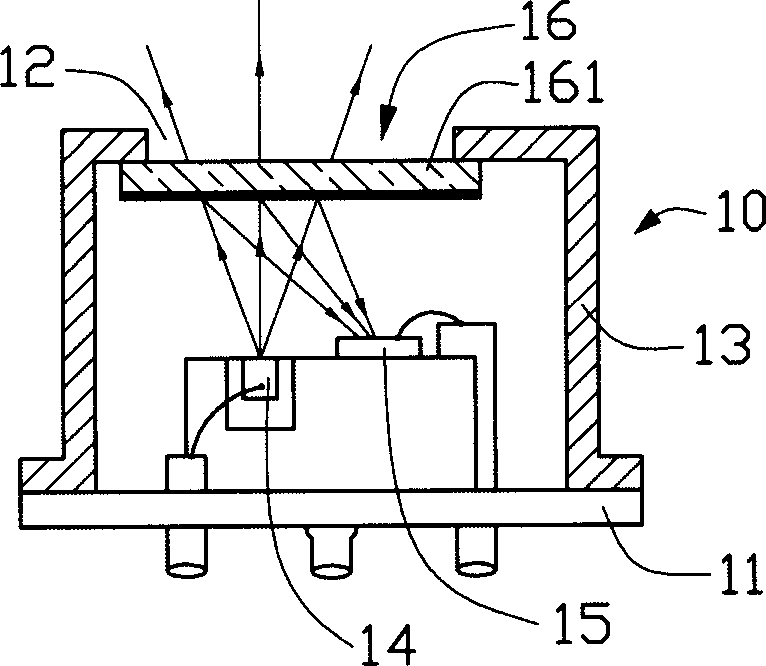
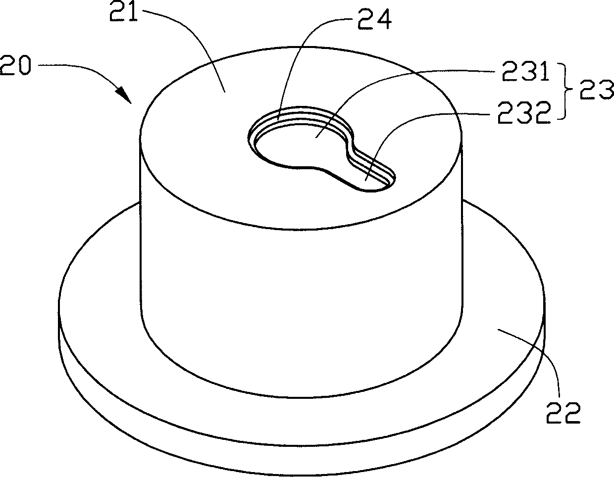
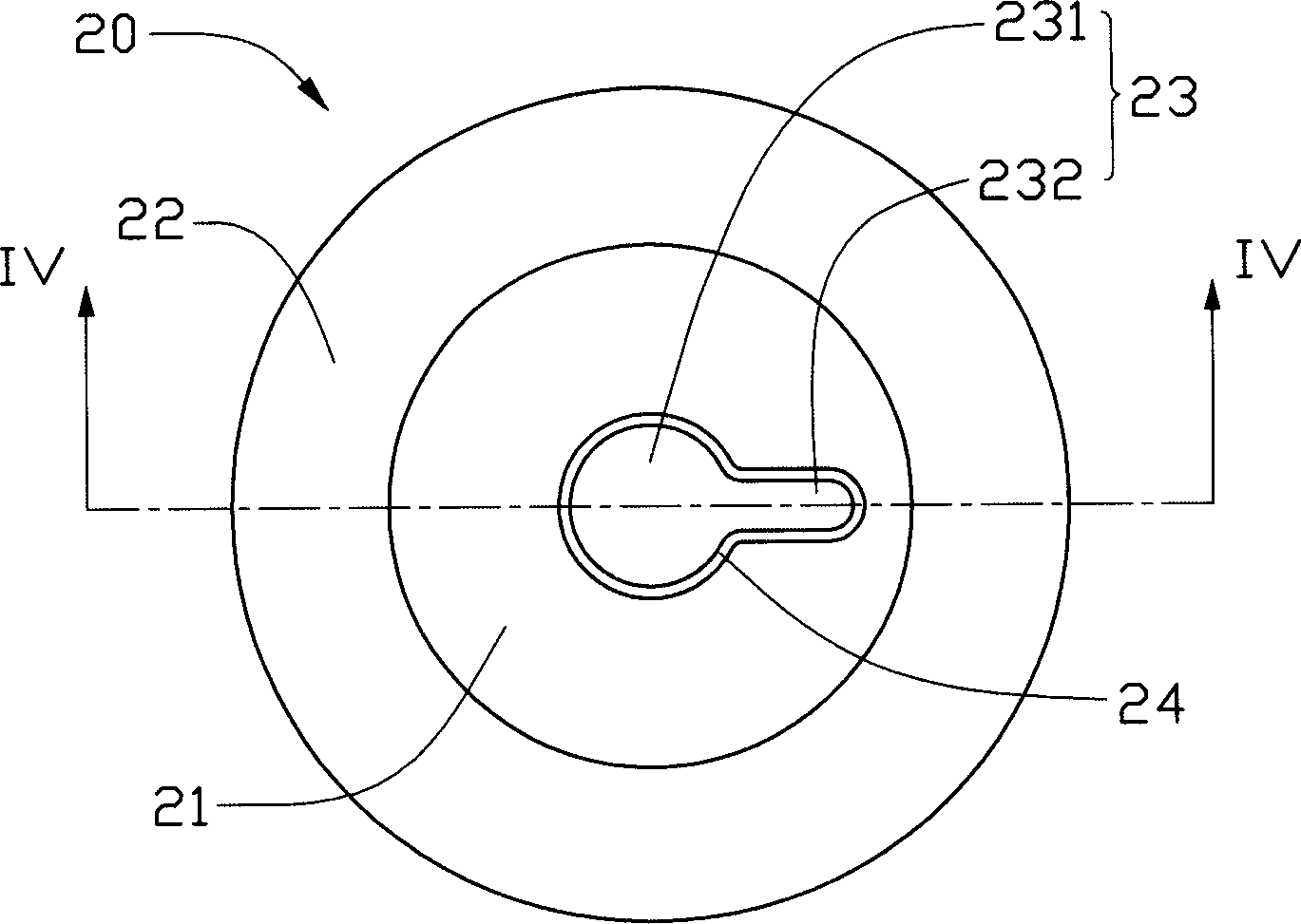
[0017] The optical device packaging cover and the manufacturing method thereof of the present invention include the steps of providing a housing and an optical lens (detailed later), please refer to figure 2 and Figure 6 As shown, the optical packaging cover 40 includes a housing 20 and an optical lens 31. The housing 20 has a flat top 21 and an annular bottom plate 22, and the housing 20 is integrally formed and substantially shaped like a pot. A through optical lens mounting portion 23 is opened on the flat top 21, and the optical lens mounting portion 23 includes a transparent opening 231 and a first-rate crossing 232. In addition, the annular bottom plate 22 is a brim-shaped annular bottom plate extending from the bottom end of the housing 20 along the edge of the housing, so that the packaging cover is connected to the base (not shown) on which the optical device is placed when the optical device (not shown) is packaged. ) Can work closely together. The housing 20 of the packaging cover can be stamped from metal material or molded by plastic.
[0018] Please refer to image 3 and Figure 4 Shown, is figure 2 The top view of the housing of the optical device packaging cover and its cross-sectional view. The edge of the light-transmitting opening 231 has a continuous rib 24. The flow passage opening 232 is an opening that passes through the light-transmitting opening 231. The rib 24 extends from the edge of the light-transmitting opening 231 to the flow passage opening 232 to form a Continuous convex ring.
[0019] Please refer to Figure 5 and Figure 6 Shown are a perspective view and a cross-sectional view of the optical device packaging cover 40 of the present invention. The optical lens 31 of the packaging cover 40 is positioned on the optical lens mounting portion 23 of the housing 20. The optical lens 31 is made of optical lens material such as transparent optical The plastic material is molded in the optical lens mounting portion 23 by an injection molding process, such as insert molding, and the convex ribs 24 of the optical lens mounting portion 23 are embedded and fixed with the flat top 21. The optical lens 31 is embedded in the flat top 21 of the housing 20 to form a light-transmitting window, which realizes the sealing and light-transmitting effects of the packaging cover 40.
[0020] The manufacturing method of the optical device packaging cover 40 of the present invention mainly includes the following steps: first, a housing 20 with a flat top 21 is provided. The housing 20 can be integrally formed by metal stamping or plastic molding, and the flat top 21 is provided with The optical lens mounting portion 23 is formed by the intersecting light-transmitting opening 231 and the flow passage opening 232. The light-transmitting opening 231 is provided with a rib 24, and the rib 24 extends from the edge of the light transmission opening 231 to the flow passage opening 232. A continuous convex ring is formed; then, a mold is provided, and the housing 20 is placed in it; an optical lens material such as a transparent optical plastic material is provided, the optical lens material is preheated and dried, and then heated to a certain viscosity, In-mold molding is used to inject the optical lens material into the closed cavity through the nozzle of the mold, and guide it to the optical lens mounting portion 23 through the runner port 232 until it is filled; after cooling and solidification, the mold is opened and taken out. The optical device package cover 40.
[0021] Please refer to Figure 7 , Is a cross-sectional view of another embodiment of the optical device packaging cover. Compared with the first embodiment, the rib 24 is replaced by an inner groove 24', and the optical lens 31' and the inner groove formed by the in-mold molding process The 24' phase is inserted into the card so as to be better held on the flat top 21 of the housing.
[0022] The transparent opening of the flat top of the housing of the optical device packaging cover of the present invention can be provided with multiple ridges or grooves, and the flow channel opening that passes through the transparent opening can be a shallow groove that does not penetrate the flat top of the housing.
[0023] The optical device packaging cover of the present invention can be used for packaging semiconductor laser diodes, light detection diodes, optical transceiver modules and the like.

PUM

no PUM

Description & Claims & Application Information

We can also present the details of the Description, Claims and Application information to help users get a comprehensive understanding of the technical details of the patent, such as background art, summary of invention, brief description of drawings, description of embodiments, and other original content. On the other hand, users can also determine the specific scope of protection of the technology through the list of claims; as well as understand the changes in the life cycle of the technology with the presentation of the patent timeline. Login to view more.

Similar technology patents

Anticoagulation coating material and preparation method thereof

InactiveCN103721300Ahigh anticoagulant activitystable structure
Owner:HUAZHONG UNIV OF SCI & TECH

High temperature-resistant and high-insulation sealing glass and preparation method thereof

ActiveCN105776868AImprove glass fluiditystable structure
Owner:XIAN SEAL ELECTRONICS MATERIAL TECH CO LTD

High-efficiency rotor for motor

InactiveCN105811625Astable structureHigh quality and safety stability
Owner:泰信电机(苏州)有限公司

Classification and recommendation of technical efficacy words

  • stable structure
  • Reduced assembly effort

Silicon/carbon composite microsphere negative electrode material as well as preparation method and application for same

ActiveCN103311522Astable structureImprove charge and discharge cycle life
Owner:INST OF PROCESS ENG CHINESE ACAD OF SCI

Preparation method of magnetic graphene based oil absorption foam material

Owner:XINJIANG TECHN INST OF PHYSICS & CHEM CHINESE ACAD OF SCI

Telescopable shaft and steering device for vehicle

InactiveCN101258335Asimple structureReduced assembly effort
Owner:JTEKT CORP +1

High-efficiency positive-pressure gas turbine

InactiveCN110094265AReduced assembly effortReduce the difficulty of assembly
Owner:JIANGSU MARITIME INST

Automatic feeding and locking assembly line for locking screw of diaphragm gas mater

ActiveCN105817874AReduced assembly effortSave assembly time
Owner:宿州市徽腾知识产权咨询有限公司

Through bolt assembling structure for square steel binding post and square steel tubular beam

PendingCN110761405Areliable qualityReduced assembly effort
Owner:BEIJING UNIVERSITY OF CIVIL ENGINEERING AND ARCHITECTURE +1

Electric motor having a rotor with a block protection sleeve, which

PendingCN114846727AEasy to assembleReduced assembly effort
Owner:SCHAEFFLER TECH AG & CO KG
Why Eureka
Try Eureka