Image sensor assembly and its mfg. method

An image sensor and component technology, applied in image communication, electrical solid-state devices, semiconductor devices, etc., can solve the problems of reducing the optical performance of the lens and expanding the refraction angle of the incident beam

Inactive Publication Date: 2003-12-24
SAMSUNG ELECTRO MECHANICS CO LTD
View PDF0 Cites 14 Cited by
  • Summary
  • Abstract
  • Description
  • Claims
  • Application Information

AI Technical Summary

Problems solved by technology

However, this conventional effort has a flaw in that it greatly expands the refraction angle of the incident beam, so that the peripheral li

Method used


Image

  • Image sensor assembly and its mfg. method
  • Image sensor assembly and its mfg. method
  • Image sensor assembly and its mfg. method

Examples


no. 2 example

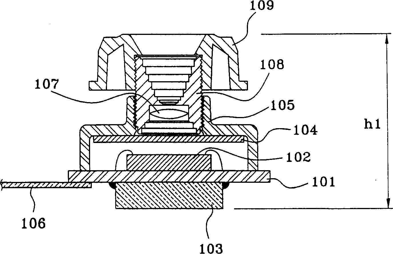
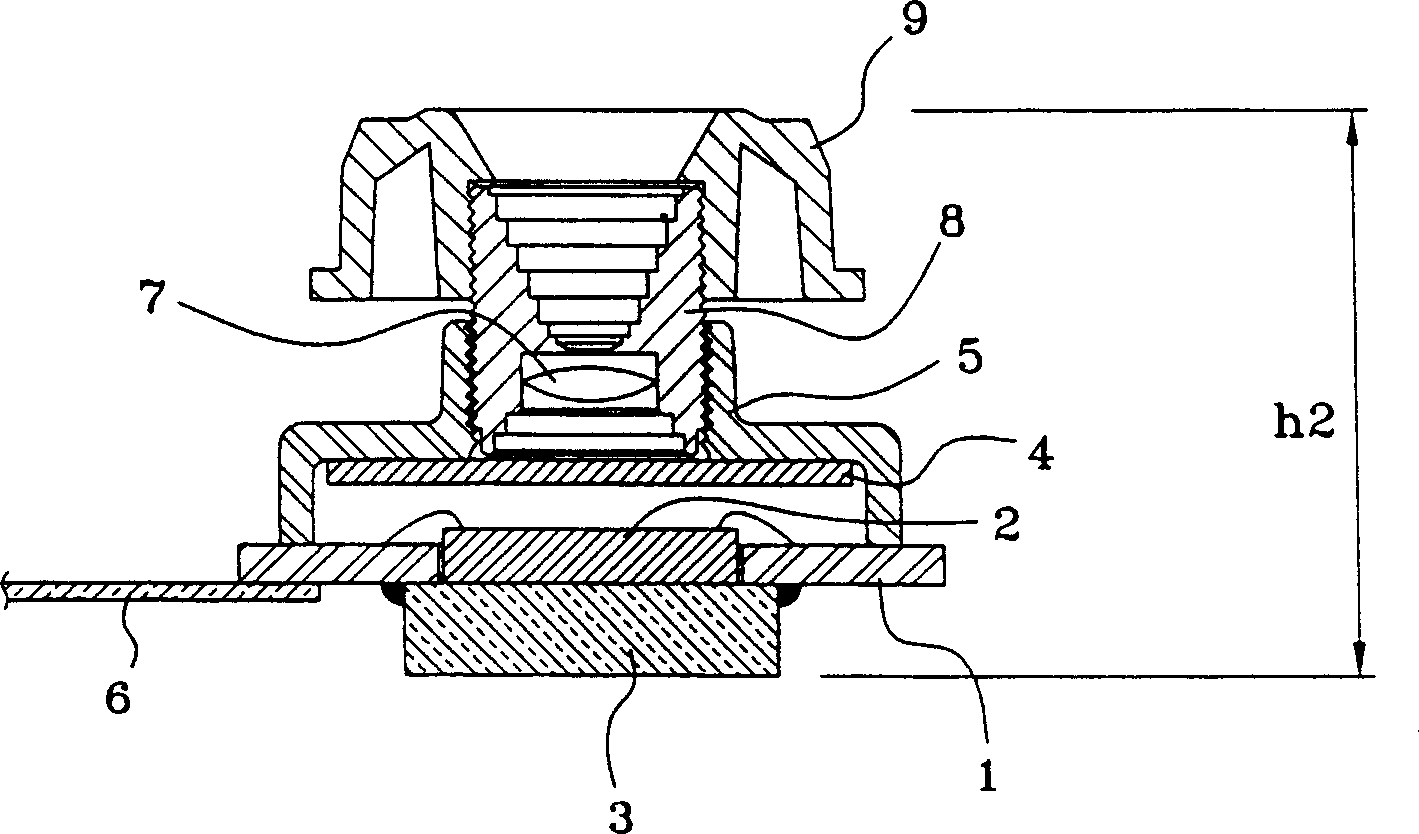
[0029] According to the second embodiment of the present invention, the camera assembly includes: an image sensor assembly, a housing 15 , a hard package 18 , a lens 17 , a knob 19 , a filter 14 and an FPCB 16 .

[0030]A hard encapsulation 18 that is threaded together is located inside the housing 15, covering the upper portion of the image sensor assembly, while a lens 17 is located within the hard encapsulation. Similar to the first embodiment, the knob 19 covers one end of the hard package, the filter 14 is located inside the housing, and the FPCB 16 is connected to the backside of the substrate 11 . At this time, the height h3 of the casing 15 of the camera module is higher than the height h2 of the casing in the first embodiment. However, the height of the camera assembly according to the second embodiment of the present invention is lower than that of the assembly in the first embodiment because the structure composed of the EMC layer 20 for sealing the back side of the...

no. 3 example

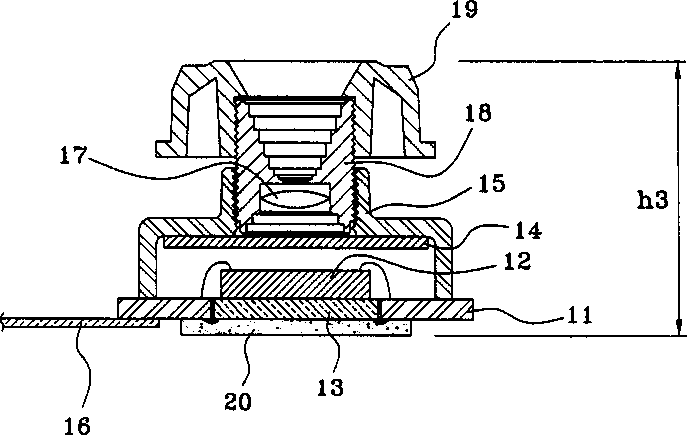
[0033] According to a third embodiment of the present invention, an image sensor assembly includes: a substrate 21 with a hole in its center; an FPCB 26 attached to the backside of the substrate 21; an ISP package 23 attached to the backside of the FPCB 26; and an image sensor 22, installed in the hole of the substrate 21.

[0034] Additionally, a camera assembly is provided. The camera assembly includes: an image sensor assembly according to the third embodiment; a housing 25 covering the upper part of the image sensor assembly; a hard package 28 engaged with threads and located inside the housing; a lens 27 located in the hard package the inner side; the knob 29, which covers one end of the hard case; and the filter, which is located on the inner side of the housing.

[0035] The process of manufacturing the image sensor assembly according to the third embodiment includes the steps of: forming a hole in the center of the substrate 21; attaching the FPCB 26 to the backside o...


PUM


Abstract

Disclosed is an image sensor module consisting of a substrate having a hole positioned at the center thereof; an image signal process package attached to the back side of the substrate; and an image sensor mounted in the hole of the substrate, and a process of fabricating the same. In addition, a camera module is provided which consists of the image sensor module; a housing covering the upper portion of the image sensor module; a lens positioned outside of the housing; a filter positioned inside of the housing; and a flexible printed circuit board connected to the back side of the substrate of the image sensor module. The image sensor module applied to the camera module can obtain a sufficient brightness while a distance between the lens and the image sensor is properly maintained to secure a desired focal distance.

Description

technical field [0001] The present invention generally relates to camera modules applied to digital cameras, and more particularly, to image sensor modules and methods of manufacturing the same. Background technique [0002] As is well known to those of ordinary skill in the art, recently, digital cameras have been widely used for Internet images and communications. In particular, as next-generation mobile communication terminals are widely used for PDAs (Personal Digital Assistants) and IMT-2000 (International Mobile Telecommunications 2000), demands for compact camera modules have increased. For example, small mobile communication terminals are being increasingly used for audio-visual communication on the Internet. In other words, there is a great demand for slim camera modules for producing digital cameras with improved functions. [0003] In particular, it is expected that a PDA terminal will be used as a multimedia device using various external devices such as a camer...

Claims


Application Information

Patent Timeline
IPC IPC(8): H01L27/14G02B7/02G06T1/00H01L23/02H01L23/12H01L31/0203H01L31/0232H04N5/225H04N5/335
CPCH01L31/0203G02B7/02H04N5/2254H01L2224/48091H01L31/0232H04N5/2253H01L31/02325H04N23/54H04N23/55H01L2924/00014H01L27/146H04N23/00H04N25/00
Inventor 金永俊崔佑荣金摞龙
Owner SAMSUNG ELECTRO MECHANICS CO LTD
Why Eureka
Try Eureka