Formation method of transistor in embedded type flash memory

An embedded, transistor technology, applied in the fields of electrical solid device, semiconductor device, semiconductor/solid state device manufacturing, etc., can solve problems such as conduction, and achieve the effect of reducing the aspect ratio

Active Publication Date: 2013-07-03
SEMICON MFG INT (SHANGHAI) CORP
View PDF7 Cites 13 Cited by
  • Summary
  • Abstract
  • Description
  • Claims
  • Application Information

AI Technical Summary

Problems solved by technology

Moreover, even when the gap 19 is not filled with conductive material, because the distance between the adjacent two contact plugs 18 is very close, the gap 19 will easily cause the adjacent two contact plugs 18 to break through the gap 19 and conduct
[0011] There are many patent documents about embedded flash memory in the prior art, such as the "method for implementing embedded flash (method for implementing flash memory device)" disclosed by the U.S. Patent Publication No. US6258667B1 published on July 10, 2001, but none Solve the above technical problems

Method used


Image

  • Formation method of transistor in embedded type flash memory
  • Formation method of transistor in embedded type flash memory
  • Formation method of transistor in embedded type flash memory

Examples


Embodiment Construction

[0053] In order to make the above objects, features and advantages of the present invention more comprehensible, specific implementations of the present invention will be described in detail below in conjunction with the accompanying drawings.

[0054] In the following description, specific details are set forth in order to provide a thorough understanding of the present invention. However, the present invention can be implemented in many other ways than those described here, and those skilled in the art can make similar extensions without departing from the connotation of the present invention. Accordingly, the present invention is not limited to the specific embodiments disclosed below.

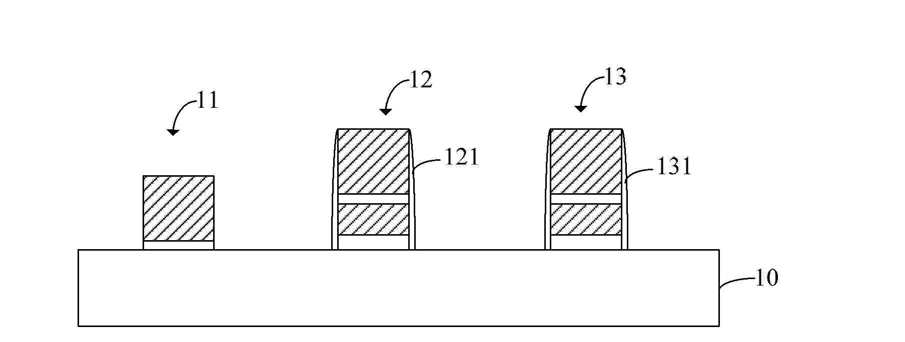
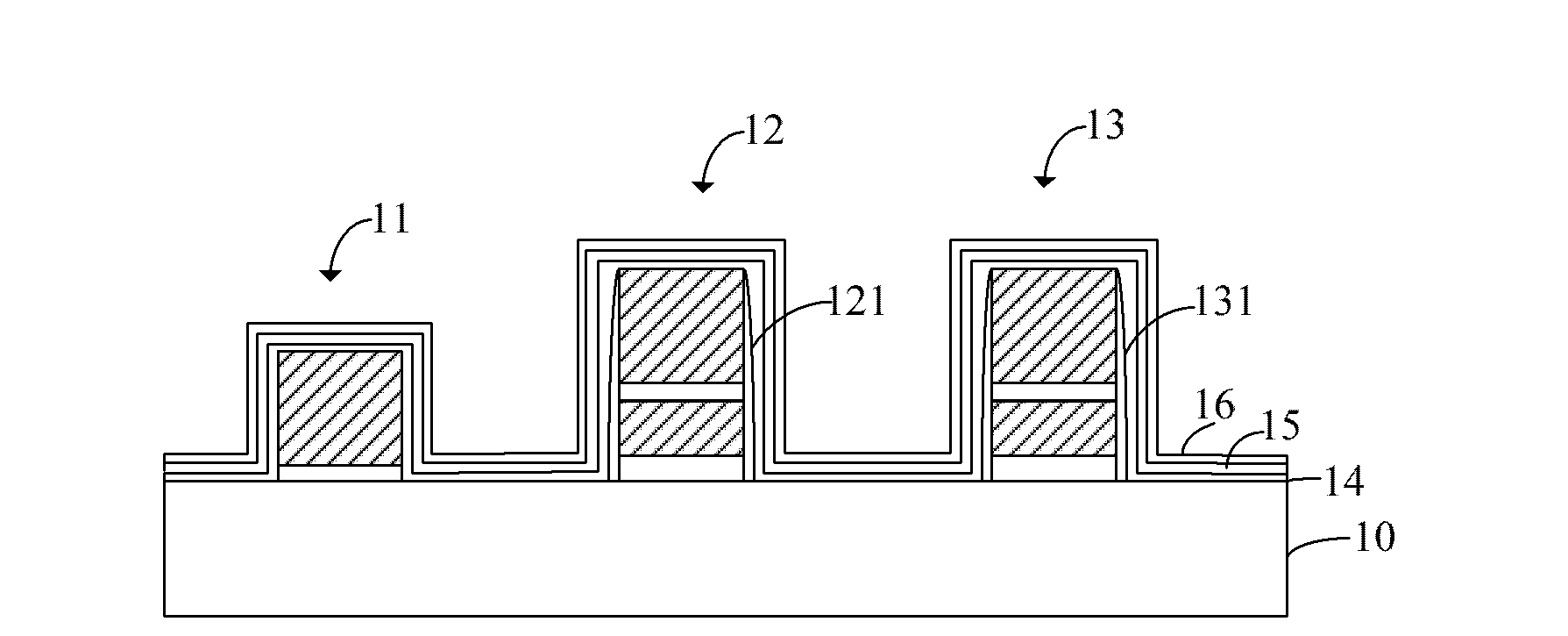
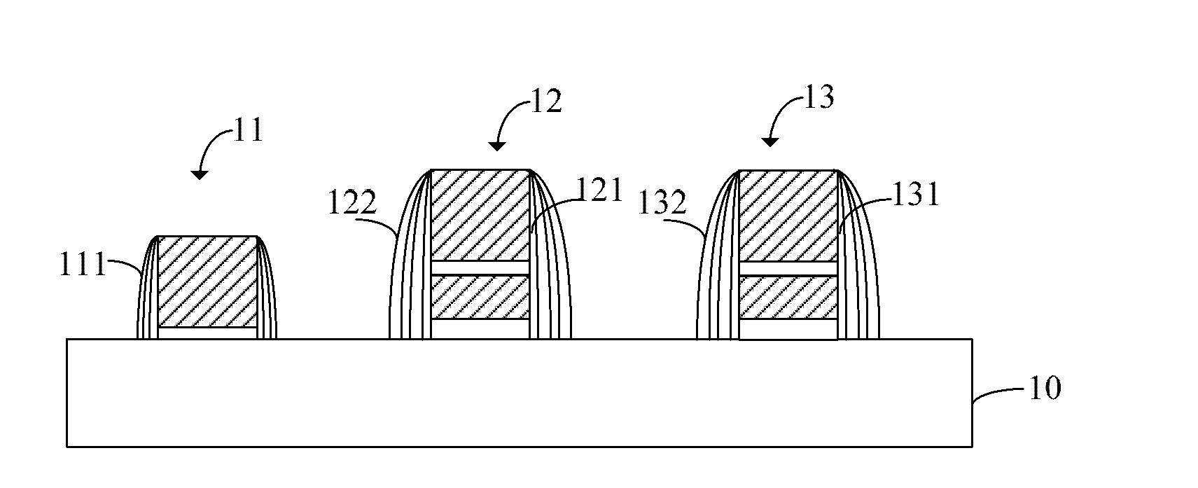
[0055] Figure 7 It is a flowchart of a method for forming a transistor in an embedded flash memory according to a specific embodiment of the present invention, refer to Figure 7 , the forming method of the transistor in the embedded flash memory of the specific embodiment of the present...


PUM


Abstract

A formation method of a transistor in an embedded type flash memory includes the following steps: a substrate with a low voltage gate structure and a storage gate structure is provided; a first dielectric layer is formed and covers the substrate, the low voltage gate structure and the storage gate structure, and then a middle side wall is formed on the periphery of the storage gate structure; a second dielectric layer is formed and covers the first dielectric layer and the middle side wall; the first dielectric layer and the second dielectric layer are etched in a dry method mode; a low voltage side wall is formed on the periphery of the low voltage gate structure, and a storage side wall is formed on the periphery of the storage gate structure; the low voltage side wall comprises an inner side wall and an outer side wall; the storage side wall comprises a middle side wall, an inner side wall and an outer side wall; the outer side wall and the middle side wall of the storage gate structure and the outer side wall of the low voltage gate structure are removed; and ion implantation is conducted, and a source electrode and a drain electrode of the low voltage gate structure and a source electrode and a drain electrode of the storage gate structure are formed. Dielectric filling capacity between layers of the storage gate structure can be increased, and the side wall width difference of a logic gate structure and the storage gate structure can also be adjusted.

Description

technical field [0001] The invention relates to the technical field of semiconductors, in particular to a method for forming a transistor in an embedded flash memory. Background technique [0002] In the current semiconductor industry, integrated circuit products can be mainly divided into three types: logic, memory and analog circuits, among which memory devices account for a considerable proportion of integrated circuit products. Among storage devices, the development of flash memory (flash memory for short) is particularly rapid in recent years. Its main feature is that it can keep stored information for a long time without power on, and has many advantages such as high integration, fast access speed, easy erasure and rewriting, etc. The field has been widely used. [0003] With the development of semiconductor technology, storage devices are more widely used, and the storage device and other device regions need to be formed on a chip at the same time to form an embedde...

Claims


Application Information

Patent Timeline
Patent Type & Authority Applications(China)
IPC IPC(8): H01L21/8247H01L27/115
Inventor 马燕春
Owner SEMICON MFG INT (SHANGHAI) CORP
Why Eureka
Try Eureka