Pellicle

A timing adjustment, circuit technology, applied to devices that give pulses at different times, televisions, optics, etc., can solve the problems of signal delay, wiring distance or different paths, etc., to achieve the effect of easy design and easy estimation

Inactive Publication Date: 2004-03-31
SEIKO EPSON CORP
View PDF0 Cites 2 Cited by
  • Summary
  • Abstract
  • Description
  • Claims
  • Application Information

AI Technical Summary

Problems solved by technology

[0004] In addition, even if positive logic signals and negative logic signals can be generated without delay between signals, if the wiring distance or path from the generating circuit to the circuit using these signals is different, it will be affected by the wiring capacity, and one signal will be relatively different from the other. one side signal delay

Method used


Image

  • Pellicle
  • Pellicle
  • Pellicle

Examples


Embodiment Construction

[0057] Hereinafter, embodiments of the present invention will be described with reference to the drawings.

[0058]

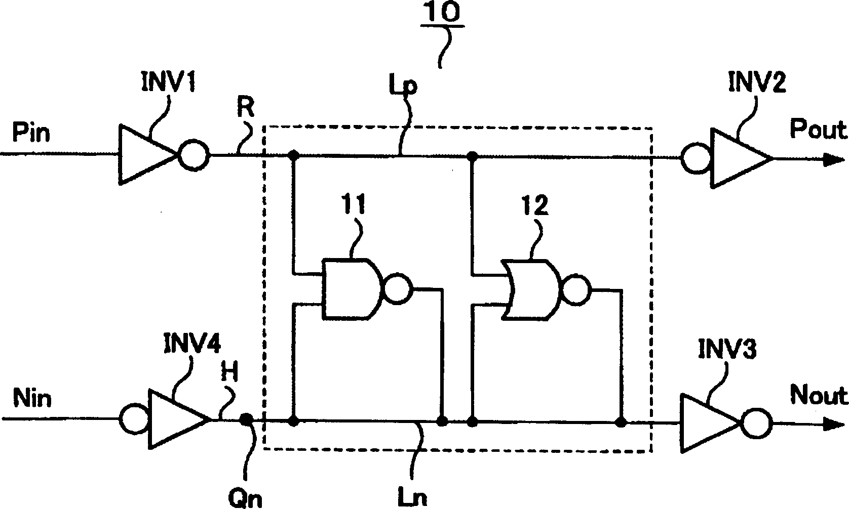
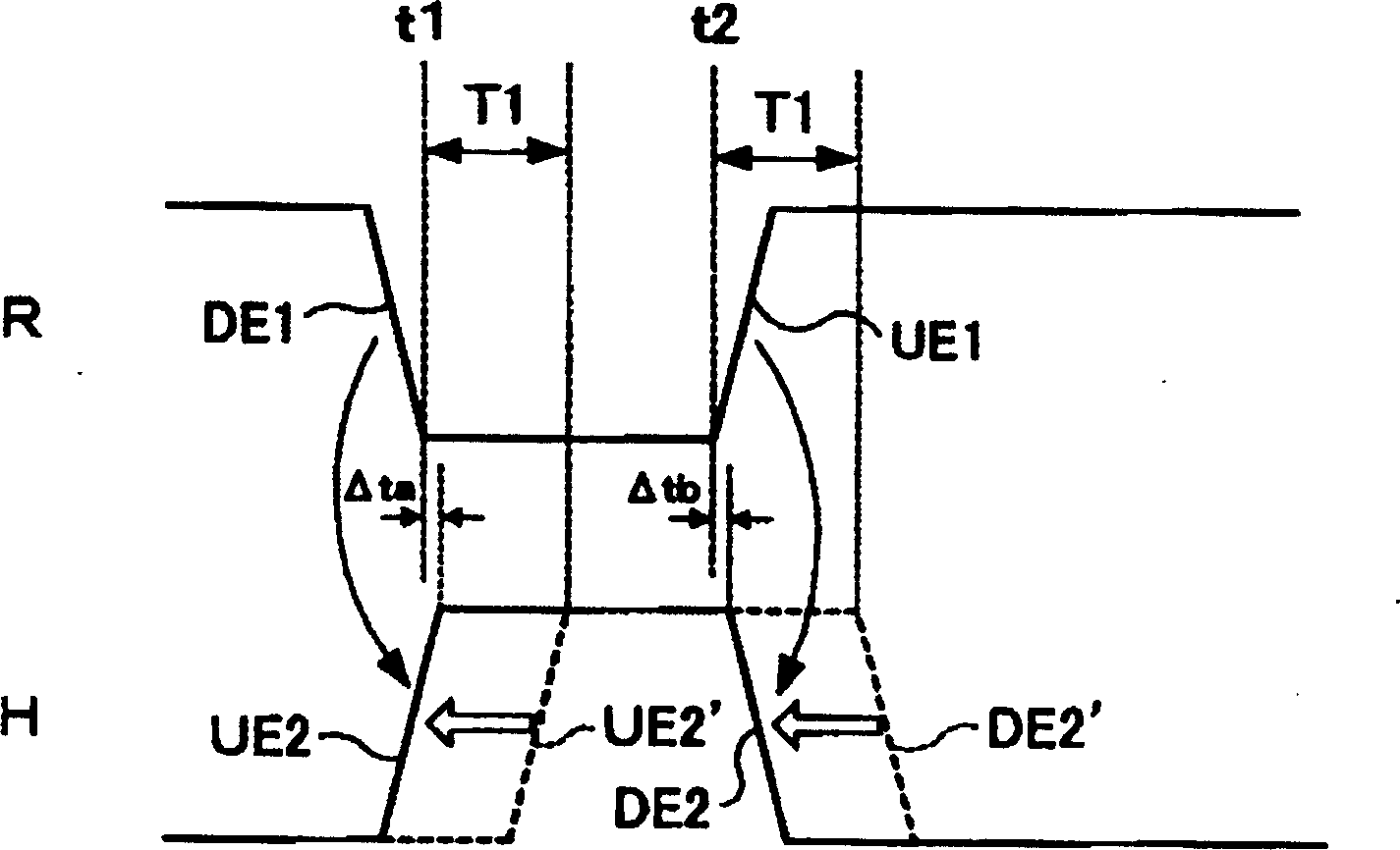
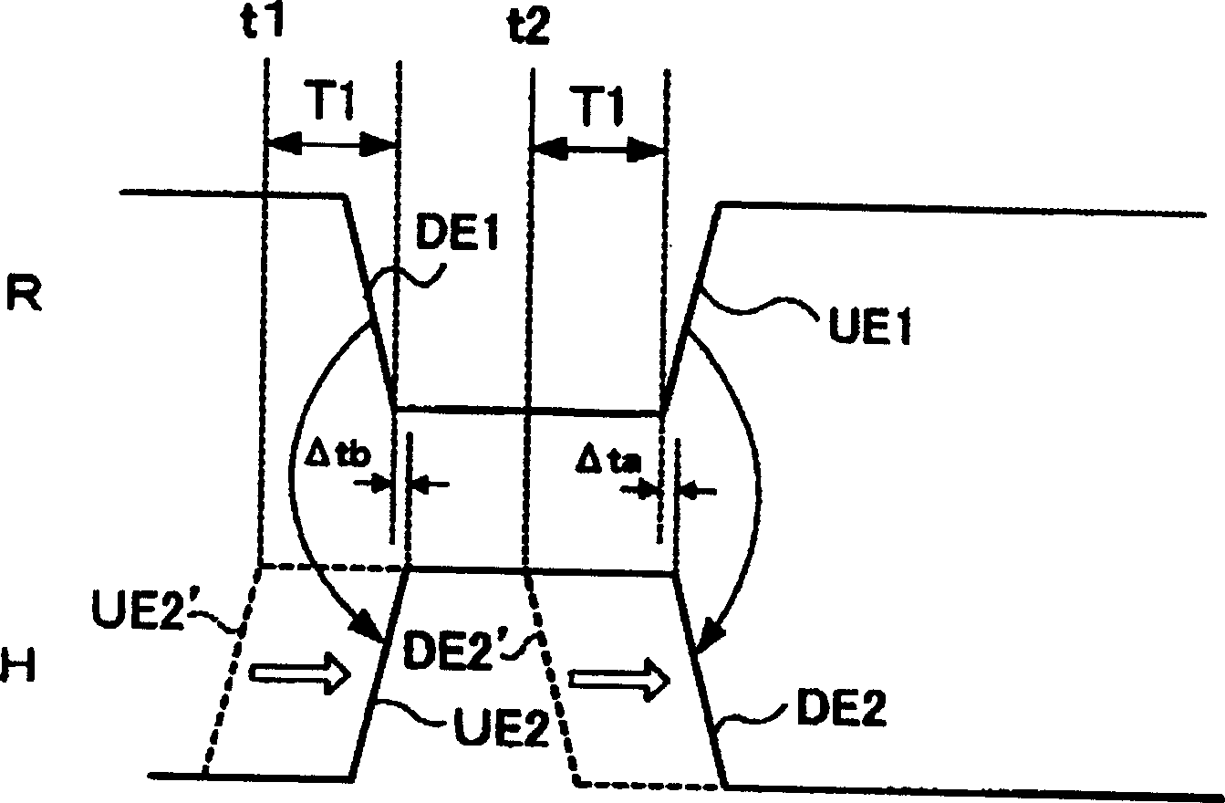
[0059] figure 1 is a circuit diagram of the timing adjustment circuit 10 . The timing adjustment circuit 10 shown in the figure includes four inverters INV1 to INV4 , a NAND circuit 11 , and a NOR circuit 12 .

[0060] The inverter INV1 inverts the input positive logic signal Pin and outputs it as a reference signal R, while the inverter INV2 inverts the input negative logic signal Nin and outputs it as a signal H to be corrected.

[0061] The output terminal of the inverter INV1 is connected to the input terminal of the inverter INV2 via the wiring Lp, and the output terminal of the inverter INV4 is connected to the input terminal of the inverter INV3 via the wiring Ln. Furthermore, a positive logic signal Pout is output from the inverter INV2, and a negative logic signal Nout is output from the inverter INV3.

[0062] One input terminal of the NAND circ...


PUM


Abstract

To facilitate the estimation of the delay time between an input and an output. Inverters INV1 and INV4 generate a reference signal R and a signal to-be-corrected H on the basis of an input positive-logic signal Pin and an input negative-logic signal Nin. Since the reference signal R is transferred through a wiring line Lp, it undergoes no delay in the process of the transfer. On the other hand, the signal to-be-corrected H undergoes the influence of the reference signal R and has its phase corrected by a NAND circuit 11 and a NOR circuit 12.

Description

technical field [0001] The present invention relates to a timing adjustment circuit, a drive circuit, an electro-optical device, and an electronic device for generating an output positive logic signal and an output negative logic signal in which the phase difference between an input positive logic signal and an input negative logic signal is reduced. Background technique [0002] Among electronic circuits, there are circuits that perform signal processing using a positive logic signal that becomes active at a high level and a negative logic signal that inverts it. As a representative circuit, there is a shift register that shifts an input pulse using a clock signal and inverting the order of the clock signal. [0003] In such an electronic circuit that operates using two-phase signals, it is desirable that there is no delay between the positive logic signal and the negative logic signal. However, there are many cases where a delay occurs between the two signals due to the g...

Claims


Application Information

Patent Timeline
Patent Type & Authority Applications(China)
IPC IPC(8): G02F1/133G02F1/136G06F11/00G09G3/20G09G3/36H03K5/00H03K5/04H03K5/151H03L7/00H04N5/66
CPCH03K5/151H03L7/00G09G3/3688G09G2320/0223G09G3/36
Inventor 藤田伸
Owner SEIKO EPSON CORP
Why Eureka
Try Eureka