Logic circuit

a logic circuit and circuit technology, applied in the field of logic circuits, can solve the problems of requiring excessive time, requiring a large number of parts, and requiring a large number of adder circuits

Inactive Publication Date: 2005-09-01
FUJITSU LTD
View PDF27 Cites 2 Cited by
  • Summary
  • Abstract
  • Description
  • Claims
  • Application Information

AI Technical Summary

Benefits of technology

[0019] It is an object of the present invention to provide a logic circuit wherein the number of kinds of basic parts is suppressed to five so that a circuit which operates at a high speed can be designed.

Problems solved by technology

First, since a look-ahead carry full adder circuit is used for an adder circuit, the adder circuit requires a great number of parts.
The reason why the look-ahead carry full adder circuit just described is used is that a carry propagation adder circuit cannot perform high speed processing.
In particular, the carry propagation adder circuit performs addition simply and propagates a carry signal successively from the lowest order figure to the highest order figure and requires excessive time for the addition.
However, since such an adder circuit or an increment circuit as described above requires many kinds of basic circuits and has a complicated structure, it has a subject to be solved in that the processing speed is low.
Further, as seen from FIG. 30, also the increment circuit includes many basic parts and has a complicated structure with a comparatively low degree of repetitiveness of wiring lines, and consequently, many man-hours are required for the layout (arrangement) of the gates and so forth.
The document 1, however, does not disclose a technique for expanding the function circuits.
Therefore, the technique of the document 2 still is complicated in construction and lacks in expandability.
However, the documents 3 to 5 do not disclose a functional circuit such as an adder circuit, a magnitude comparison circuit, an increment circuit or a like circuit.
However, the documents 6 and 7 are directed toward providing an EXOR or EXNOR circuit which requires a smaller number of transistors than an ordinary device and providing a CMOS full adder stage in which such an EXOR or EXNOR circuit is used, and do not disclose a technique relating to high speed operation or expandability.
In addition, the documents mentioned above do not disclose any technique for saving time required for tuning (adjustment) of components.
In particular, where a great number of components are involved, there is a subject to be solved in that much time is required for tuning of the components.

Method used


Image

  • Logic circuit
  • Logic circuit
  • Logic circuit

Examples


first embodiment

A. First Embodiment of the Invention

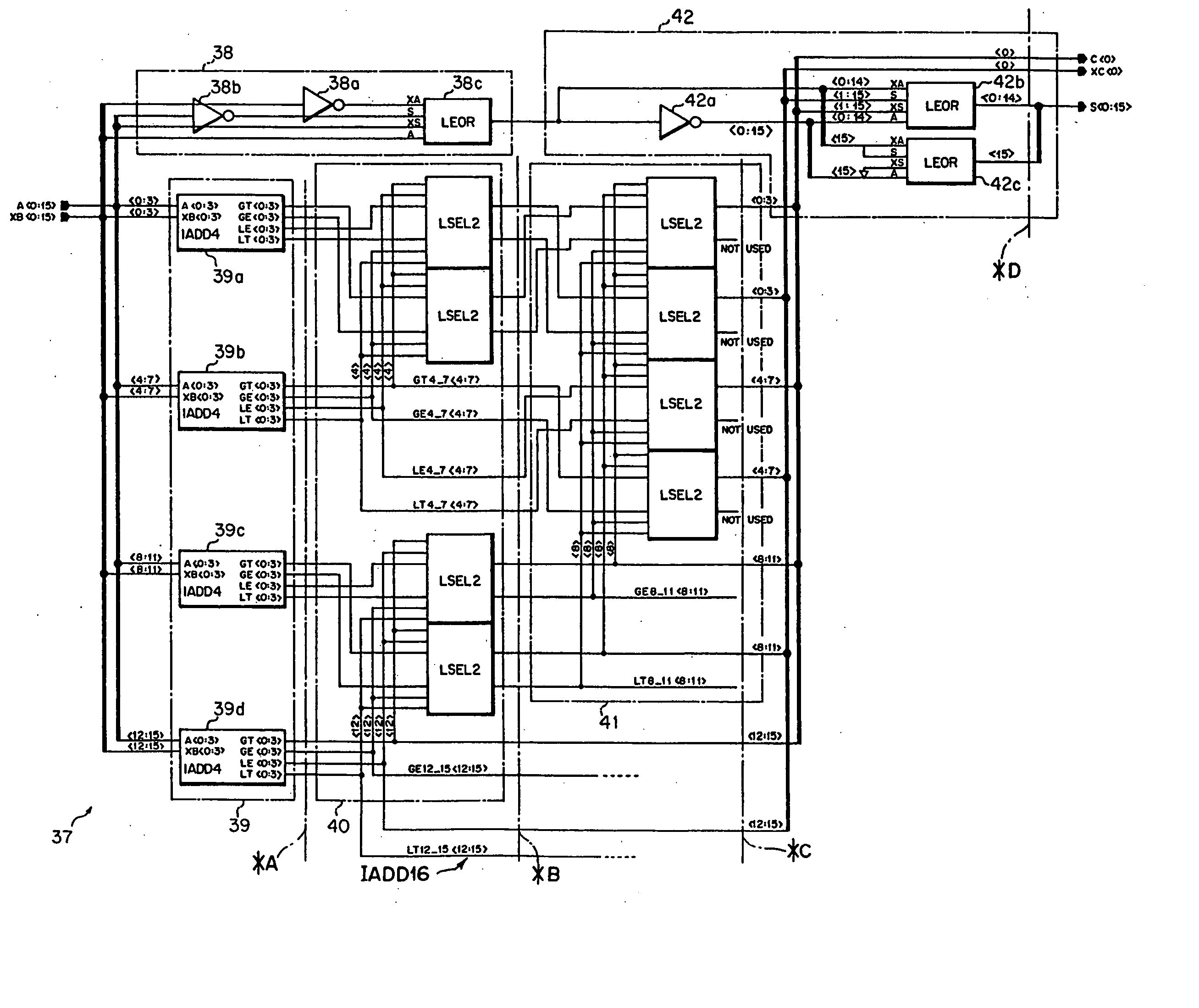
[0075]FIG. 1 is a block diagram showing a construction of a first leaf cell according to an embodiment of the present invention. Referring to FIG. 1, the cell LEOR shown is a CMOS logic circuit composed of a first inversion section 1a, a second inversion section 1b, and a transmission section 1c, and has terminals A, XS, S, XA and X.

[0076] The first inversion section 1a inverts a first input signal having one of positive logic and negative logic and outputs the inverted signal. The first inversion section 1a includes two CMOS logics 1aa and 1ab connected in parallel. A signal inputted from the terminal A is inputted to the transistor gates of the two CMOS logics 1aa and 1ab. When the input signal from the terminal A is 1, a gate T1 has an off state and a gate T2 has an on state, and a signal line P100 has a ground potential. On the other hand, when the input signal from the terminal A is 0, the gate T1 is on and the gate T2 is off, and the signal...


PUM


Abstract

A CMOS logic circuit is disclosed wherein the number of kinds of basic parts is suppressed to five to allow designing of a circuit which operates at a high speed and repetitiveness of wiring lines is increased to allow designing of a circuit which is simple in circuit scale and high in expandability and besides the time required for adjustment of components is reduced significantly to reduce the man-hours for arrangement significantly to reduce the man-hours for development significantly and the same basic parts are used so as to achieve augmentation of the yield and promote reduction of the production cost. A basic cell of the CMOS logic circuit includes a first inversion section for inverting a first input signal having one of positive logic and negative logic and outputting the inverted signal, a second inversion section for inverting a second input signal having the other of the positive logic and the negative logic and outputting the inverted signal, and a transmission section for selectively outputting one of the output of the first inversion section and the output of the second inversion section in accordance with a logical value which depends upon an externally controllable selection signal and an inverted signal of the selection signal.

Description

BACKGROUND OF THE INVENTION [0001] 1) Field of the Invention [0002] This invention relates to a logic circuit suitable for use with a magnitude comparison circuit, a carrier production circuit, a full adder circuit and an increment circuit. [0003] 2) Description of the Related Art [0004] A great number of magnitude comparison circuits, carry generation circuits, full adder circuits and increment circuits are used as basic circuits in a processor. The processor requires a large number of basic circuits in order to perform addition and subtraction with operation commands. For example, a magnitude comparison circuit is used for floating point arithmetic. In particular, when floating point arithmetic is performed, positioning of two parts including a characteristic and a mantissa of a numeral must be performed. Therefore, the magnitude comparison circuit is used when it is required to compare two parts of a numeral to discriminate which one of the two parts is a characteristic or a mant...

Claims


Application Information

Patent Timeline
Patent Type & Authority Applications(United States)
IPC IPC(8): G06F7/50G06F7/02G06F7/42G06F7/501G06F7/505G06F7/506G06F7/508H03K17/693H03K19/0948H03K19/20
CPCG06F7/026G06F7/5055H03K19/20H03K17/693G06F7/506
Inventor KATAKURA, HIROSHINAKASHIMA, YASUHIKO
Owner FUJITSU LTD
Why Eureka
Try Eureka