Semiconductor device

a technology of semiconductor devices and semiconductors, applied in semiconductor devices, digital storage, instruments, etc., can solve the problems of poor connection, easy problem, and need for control circuits to be added, so as to prevent the yield from decreasing and reduce the number of connections

Inactive Publication Date: 2006-01-05
PANASONIC CORP
View PDF3 Cites 2 Cited by
  • Summary
  • Abstract
  • Description
  • Claims
  • Application Information

AI Technical Summary

Benefits of technology

[0026] The present invention is provided in order to solve the above described problems with the prior art, and an object thereof is to provide a semiconductor device which makes it possible to change the logic while restricting the increase in the number of circuits, in a manner where the

Problems solved by technology

Furthermore, it becomes easy for the problem of poor connection to occur in the steps for wiring and in the steps for creating via holes for the connection between the drains of memory cell transistors and bit lines, due to miniaturization of the processed object.
However, a problem arises where a control circuit must be added.
In addition, there is a problem where it is difficult to control information at the time of analysis, whether or not the drains of

Method used


Image

  • Semiconductor device
  • Semiconductor device
  • Semiconductor device

Examples


first embodiment

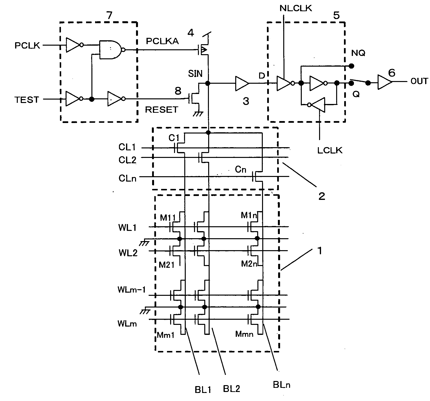
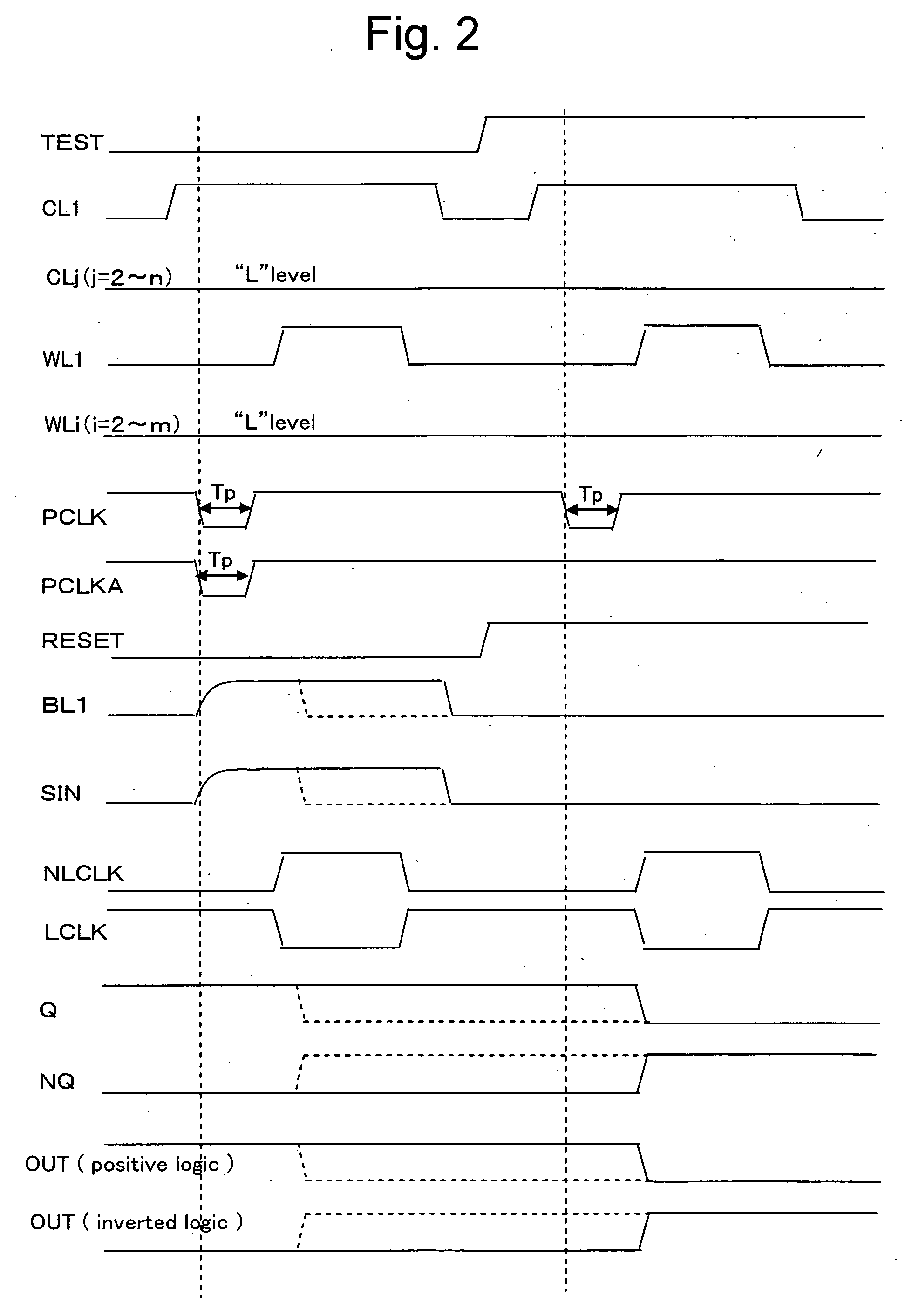
[0067]FIG. 1 is a circuit diagram showing the configuration of a semiconductor device, that is to say, a mask ROM, according to the first embodiment of the present invention.

[0068] The semiconductor device of this embodiment is, as shown in FIG. 1, formed of a memory cell array 1, a column decoder 2, a sense amplifier 3, a transistor for charging 4, a latch circuit 5, an output buffer circuit 6, a charge signal control circuit 7 and a transistor for discharging 8. Memory cell array 1, column decoder 2, sense amplifier 3, transistor for charging 4 and output buffer circuit 6 are the same as those in the prior art, and therefore, the same symbols are attached to the same components, and the descriptions thereof are omitted.

[0069] Latch circuit 5, of which the input terminal is connected to the output of sense amplifier 3, outputs a signal in the same logic as that of an input D to an output terminal Q, and outputs a signal in the negative logic to an output terminal NQ when a latch ...

second embodiment

[0083]FIG. 3 is a circuit diagram showing the configuration of a semiconductor device, that is to say, a mask ROM, according to the second embodiment of the present invention.

[0084] The semiconductor device of this embodiment is, as shown in FIG. 3, formed of a memory cell array 1, a column decoder 2, a sense amplifier 3, a transistor for charging 4, a latch circuit 5, an output buffer circuit 6 and a column signal control circuit 9. Memory cell array 1, column decoder 2, sense amplifier 3, transistor for charging 4, latch circuit 5 and output buffer circuit 6 are the same as those in the prior art and in the first embodiment, and therefore, the same symbols are attached to the same components, and descriptions thereof are omitted. In addition, the semiconductor device of the present embodiment is also provided with a test terminal (not shown) into which a test control signal TEST is inputted from the outside.

[0085] Column signal control circuit 9, into which column selection sign...

third embodiment

[0094]FIG. 5 is a circuit diagram showing the configuration of a semiconductor device, that is to say, a mask ROM, according to the third embodiment of the present invention.

[0095] The semiconductor device of this embodiment is, as shown in FIG. 5, formed of a memory cell array 1, a column decoder 2, a sense amplifier 3, a transistor for charging 4, a latch circuit 5, an output buffer circuit 6 and a word line control circuit 10. Memory cell array 1, column decoder 2, sense amplifier 3, transistor for charging 4, latch circuit 5 and output buffer circuit 6 are the same as those in the prior art and in the first embodiment, and therefore, the same symbols are attached to the same components, and descriptions thereof are omitted. In addition, the semiconductor device of the present embodiment is also provided with a test terminal (not shown) into which a test control signal TEST is inputted from the outside.

[0096] Word line control circuit 10, into which word line selection signals ...


PUM


Abstract

An output end and an inverted output end of a latch circuit that is connected to an output buffer circuit are switched with each other, and thereby, the relationship between the data of “0” or “1” and the drain of a memory cell is connected or not connected to a bit line is changed. In addition, an input of a sense amplifier is fixed at the grounding potential by means of a test control signal, and thereby, positive logic is confirmed in the case where the output of the output buffer circuit is “L,” and negative logic is confirmed in the case where the output of the output buffer circuit is “H.”

Description

BACKGROUND OF THE INVENTION [0001] 1. Field of the Invention [0002] The present invention relates to a semiconductor device with a mask ROM (mask programmable ROM) which is programmable by means of a mask. [0003] 2. Prior Art [0004] Patent Document 1, for example, discloses a conventional semiconductor device. Paragraphs 0002 to 0006 on page 2 and FIG. 2 of this document disclose the configuration of a contact programming mask ROM. [0005]FIG. 9 is a circuit diagram showing the configuration of the above described contact programming mask ROM. In a contact programming ROM, whether or not the drain of a memory cell transistor is connected to a bit line respectively corresponds to “0” or “1” of memory data. Such a mask ROM is programmable by means of a mask. [0006] A conventional semiconductor device is, as shown in FIG. 9, formed of a memory cell array 1, a column decoder 2, a sense amplifier 3, a transistor for charging 4, an output buffer circuit 6 and a latch circuit 15. [0007] Mem...

Claims


Application Information

Patent Timeline
IPC IPC(8): G11C7/00G11C7/10G01R31/28G11C17/00G11C17/12G11C17/18G11C29/00G11C29/14H01L21/8246H01L27/10H01L27/112
CPCG11C17/14G11C29/1201G11C29/14G11C2029/1202G11C17/12G11C7/1051G11C7/106G11C7/1069G11C2029/1204
Inventor NAKAYA, SHUJIHAYASHI, MITSUAKIKURATA, MASAKAZU
Owner PANASONIC CORP
Why Eureka
Try Eureka