Method of removing photoresist layer and method of fabricating semiconductor device using the same

a technology of photoresist layer and fabrication method, which is applied in the direction of photomechanical treatment, instruments, electrical equipment, etc., can solve the problems of contaminating the machine or yielding the substrate, and achieve the effect of effectively removing the photoresist layer and avoiding contamination of the machin

Inactive Publication Date: 2008-10-23
UNITED MICROELECTRONICS CORP
View PDF9 Cites 20 Cited by
  • Summary
  • Abstract
  • Description
  • Claims
  • Application Information

AI Technical Summary

Benefits of technology

[0008]The present invention provides a method of effectively removing a photoresist layer so as t

Problems solved by technology

Thereby, the irremovable photoresist fragments 10a may result i

Method used


Image

  • Method of removing photoresist layer and method of fabricating semiconductor device using the same
  • Method of removing photoresist layer and method of fabricating semiconductor device using the same
  • Method of removing photoresist layer and method of fabricating semiconductor device using the same

Examples


example 1

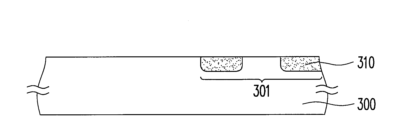
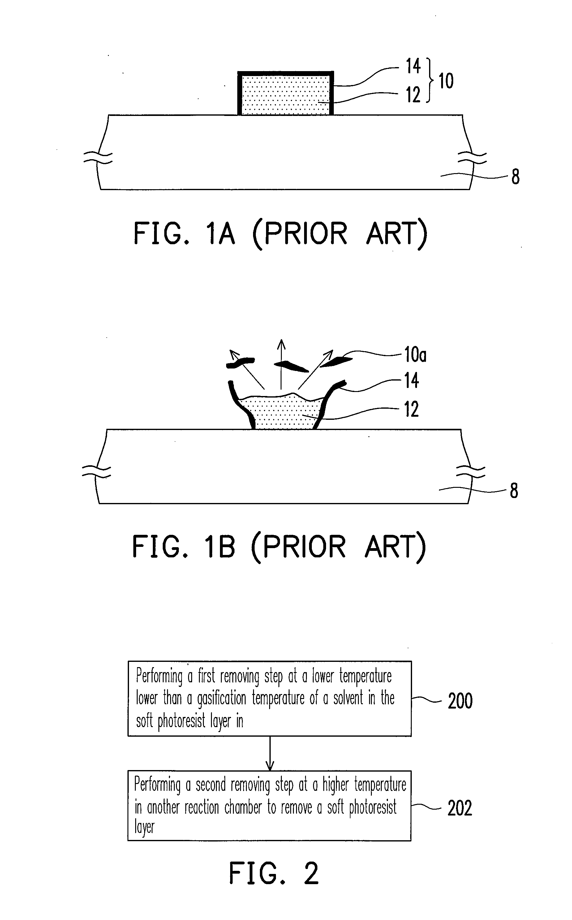
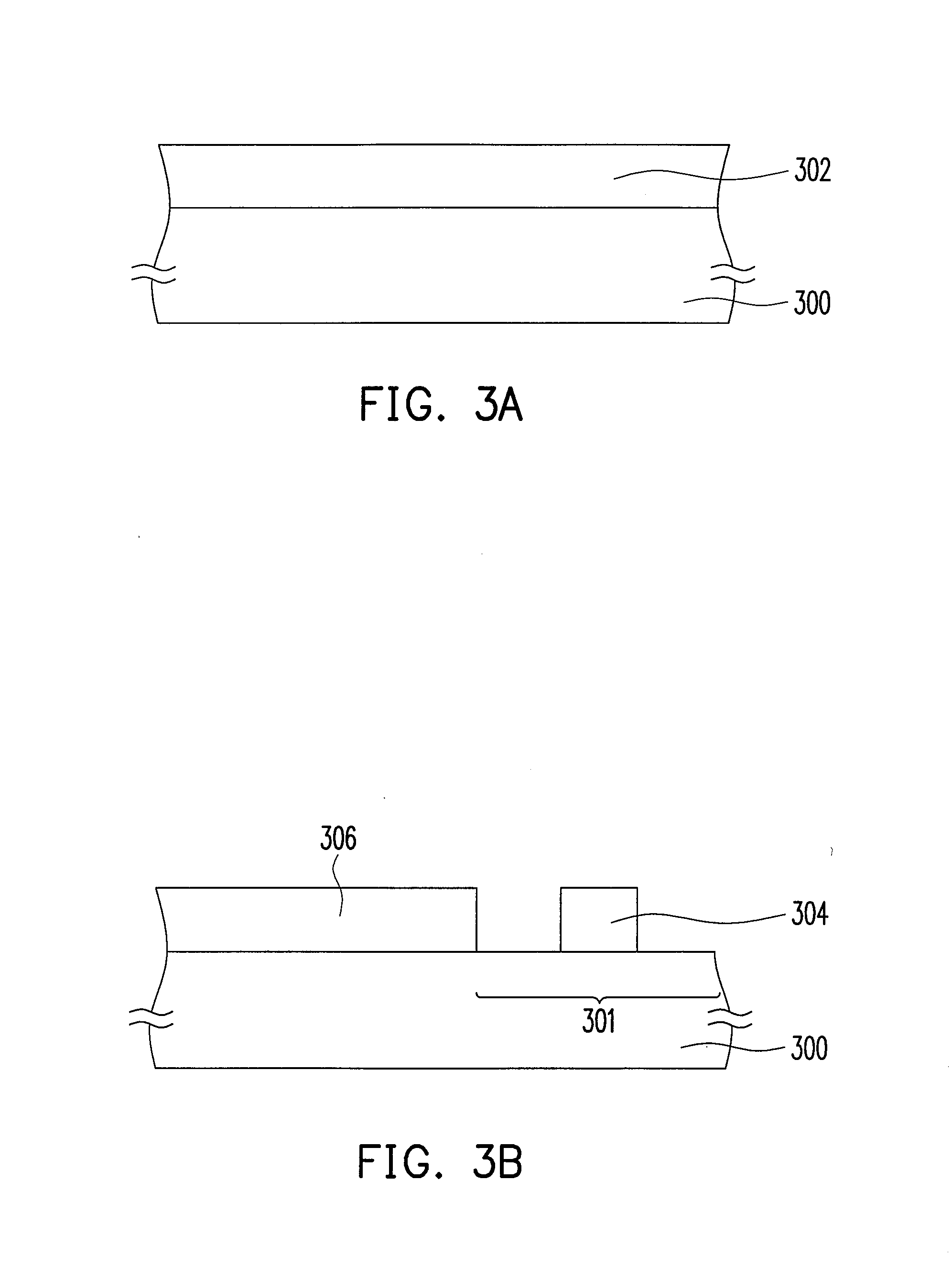
[0060]A substrate is provided. A patterned photoresist layer is already formed on the substrate, and an ion implantation process is already performed thereon. Next, a first removing step is performed in a first chamber of a plasma machine in a pinning-down manner. A temperature at which the first removing step is performed is 90° C. Gases adopted in said step is O2 and N2H2. A pressure thereof is 5 torr. Thereafter, a second removing step is performed in a different chamber of the same plasma machine The temperature at which the second removing step is performed is 250° C. The gases adopted in said step is O2 and N2H2. The pressure thereof is 5 torr. Afterwards, defects on the substrate are measured. Finally, a cleaning process is performed, and the defects on the substrate are again measured. The test results are shown in table 1. Comparative Example 1 is performed using the prior art method.

TABLE 1ComparativeExample 1Example 1Sample 1Sample 2Sample 3Sample 1Sample 2Post strip23652...


PUM


Abstract

A method of removing a photoresist layer is provided. An ion implantation process has been performed on the photoresist layer to transform a surface of the photoresist layer to a crust and a soft photoresist layer remains within the crust. The method includes performing a first removing step to remove the crust, such that the soft photoresist layer is exposed. Thereafter, a second removing step is performed to remove the soft photoresist layer. The first and the second removing steps are performed in difference chambers, and a temperature for performing the first removing step is lower than that for performing the second removing step and lower than a gasification temperature of a solvent in the soft photoresist layer.

Description

BACKGROUND OF THE INVENTION[0001]1. Field of the Invention[0002]The present invention relates to a method of fabricating an integrated circuit, and more particularly to a method of removing a photoresist layer and a method of fabricating a semiconductor device using the same.[0003]2. Description of Related Art[0004]In a process of manufacturing semiconductors, a great number of integrated circuits are frequently formed on substrates. A plurality of electronic devices such as transistors, diodes, capacitors, resistors and the like is often included in the integrated circuits. Fabrication of the electronic devices usually involves depositing, removing, and implanting ions at certain locations which can be facilitated by a photolithography process.[0005]The photolithography process includes depositing a layer of photoresist material on a substrate at first. Then, patterns on a photomask are transferred to the photoresist material layer after being exposed to radiation passing through t...

Claims


Application Information

Patent Timeline
IPC IPC(8): H01L21/425G03C5/00
CPCG03F7/427H01L21/31133H01L21/31138
Inventor SUN, ZHI-QIANGPEI, XILAN, TIEN-CHENGCHEN, YU-JOUZHOU, GUO-FUHUANG, KAI-PINGGAN, HONG-SIEKYAN, JIAN-PENGYANG, KAIZHANG, SHENG
Owner UNITED MICROELECTRONICS CORP
Why Eureka
Try Eureka