Semiconductor device and producing method thereof

A manufacturing method and semiconductor technology, which is applied in the field of semiconductor devices and semiconductor device manufacturing, can solve problems such as the bad influence of gate insulating films, and achieve the effect of miniaturization

Inactive Publication Date: 2004-04-21
KK TOSHIBA
View PDF1 Cites 1 Cited by
  • Summary
  • Abstract
  • Description
  • Claims
  • Application Information

AI Technical Summary

Problems solved by technology

However, in this case, since the side walls of the formed trench also include the side surfaces of the gate insulating film, it must be taken into account not to adversely affect the gate insulating film.

Method used


Image

  • Semiconductor device and producing method thereof
  • Semiconductor device and producing method thereof
  • Semiconductor device and producing method thereof

Examples


Embodiment Construction

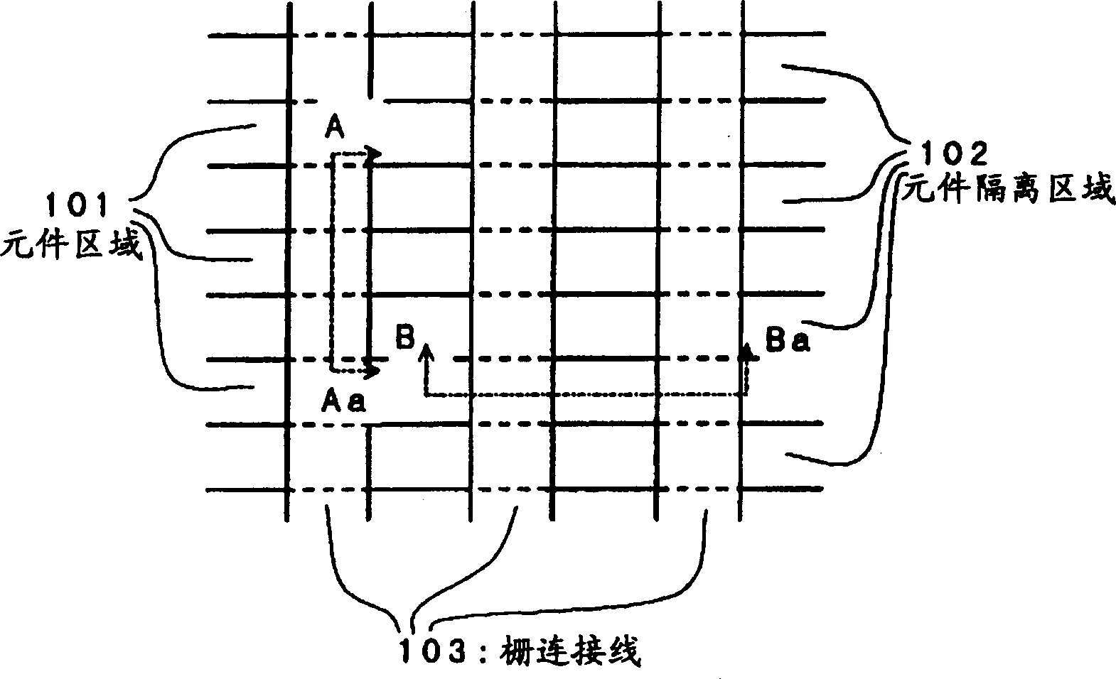
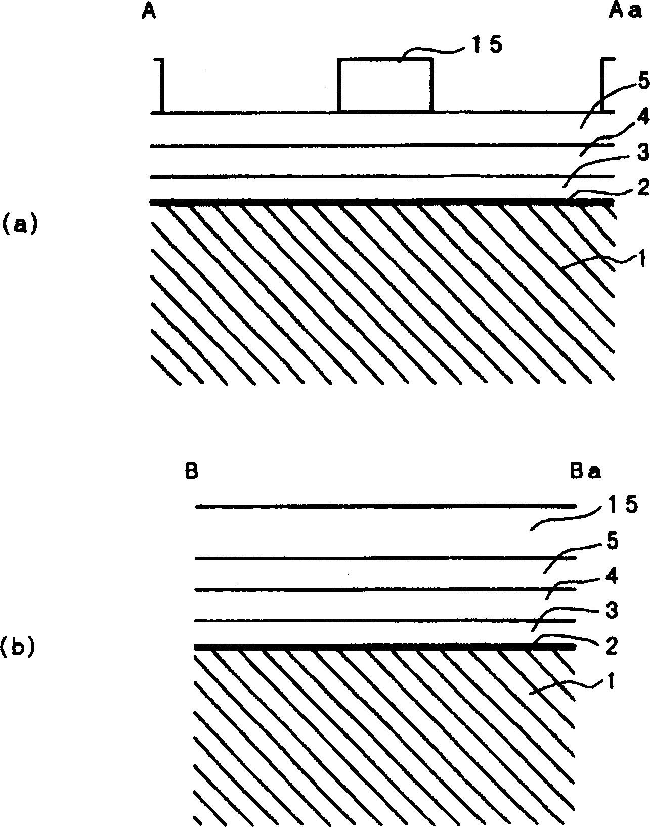
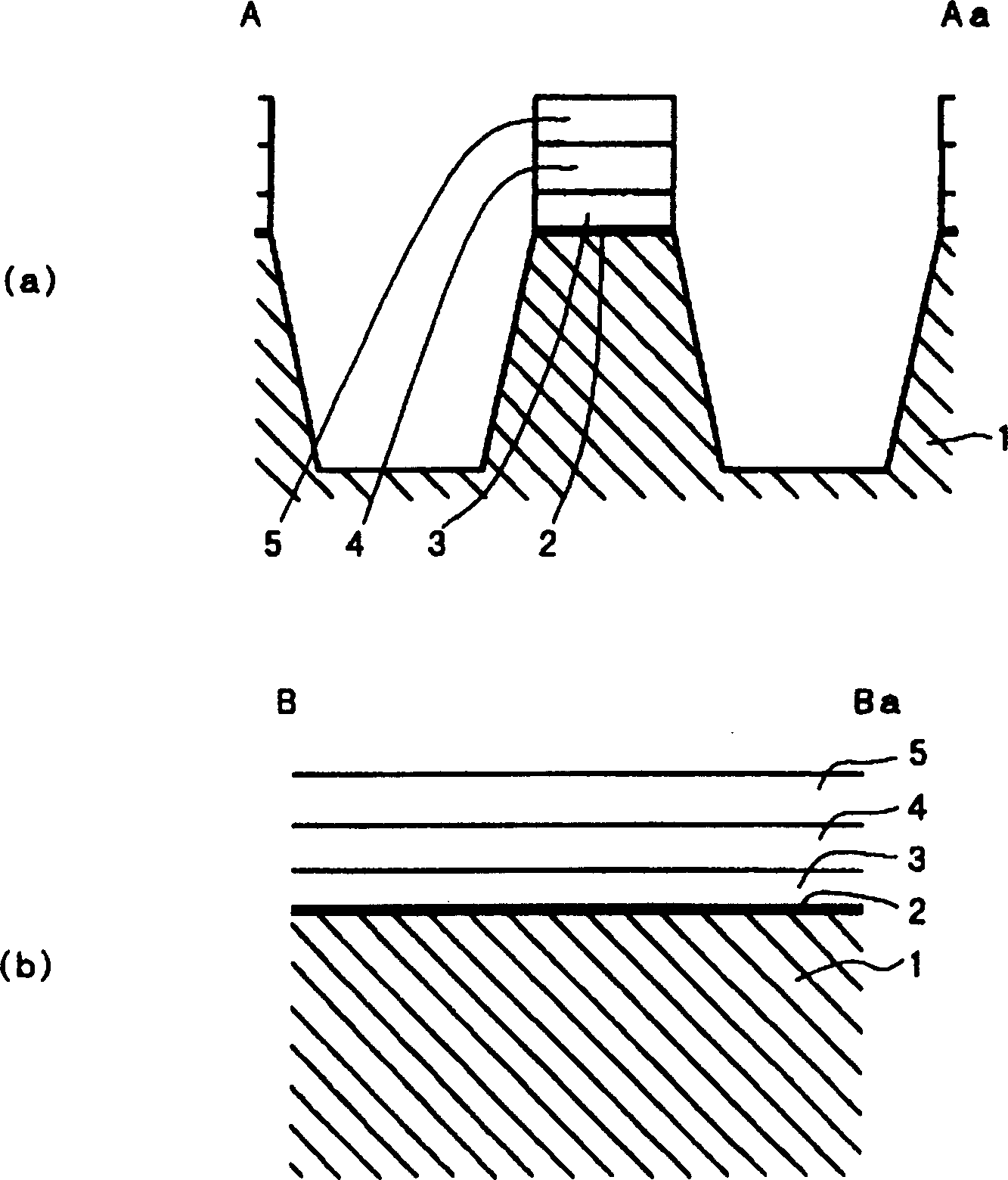
[0034] Based on the above, a nonvolatile semiconductor memory as an example of an embodiment of the present invention will be described below with reference to the drawings. figure 1The plan view of FIG. 2 schematically shows the configuration of a nonvolatile semiconductor memory according to an embodiment of the present invention. As shown in the figure, in this nonvolatile semiconductor memory, cells (MOS transistors having floating gate electrodes) serving as memory elements are arranged in an array.

[0035] That is, element regions 101 and element isolation regions 102 that isolate these element regions 101 are alternately arranged in stripes, and one element region 101 has a plurality of cells in the left-right direction in the figure. In the direction perpendicular to the direction in which the element region 101 extends, the gate connection lines 103 connecting the control gate electrodes are also formed in stripes.

[0036] A floating gate electrode (not shown) is b...


PUM


Abstract

In a semiconductor device including a plurality of element regions and an element isolation region based on STI (shallow trench isolation) which electrically isolates the element regions from each other, each of the element regions includes; a channel region; source/drain regions formed to sandwich the channel region in a horizontal direction; a gate insulation film which is formed on the channel region and in which an angle of a bird's beak is 1 degree or smaller, the bird's beak being formed from a side of the element isolation region on a surface opposite a surface facing the channel region in a horizontal direction substantially perpendicular to the direction in which the source/drain region sandwich the channel region; and a gate electrode layer formed on the gate insulation film.

Description

technical field [0001] The present invention relates to a semiconductor device having a field effect transistor including a gate insulating film and a method for manufacturing the same, and more particularly to a semiconductor device suitable for further miniaturization of the transistor size and a method for manufacturing the same. Background technique [0002] In a structure that can be used in a semiconductor device integrating field effect transistors provided with a gate insulating film, and in a structure in which regions where these transistors are provided are electrically isolated from each other (element isolation), for example, there is JP-A-9 - Construction described in bulletin No. 181166. This gazette describes a structure in which, instead of using selective oxidation, a trench is formed on a substrate and an oxide is buried in the trench for element isolation. [0003] [Patent Document 1] [0004] Japanese Patent Application Publication No. 9-181166 [000...

Claims


Application Information

Patent Timeline
Patent Type & Authority Applications(China)
IPC IPC(8): H01L21/76H01L21/762H01L21/8234H01L21/8247H01L27/115H01L29/78H01L29/788H01L29/792
CPCH01L21/823481H01L21/76224H01L21/823462H01L21/76
Inventor 园田真久井口直角田弘昭坂上荣人
Owner KK TOSHIBA
Why Eureka
Try Eureka