Integrated circuit self-testing method based on electric programmed three-D memory

An integrated circuit and memory technology, applied in the field of electrical programming three-dimensional integrated memory, can solve the problems of 3D-M read and write speed, yield programmability, etc.

Inactive Publication Date: 2004-05-19
张国飙
View PDF3 Cites 2 Cited by
  • Summary
  • Abstract
  • Description
  • Claims
  • Application Information

AI Technical Summary

Problems solved by technology

Standalone 3D-M needs to be improved in terms of read and write speed, yield, programmability, etc.

Method used


Image

  • Integrated circuit self-testing method based on electric programmed three-D memory
  • Integrated circuit self-testing method based on electric programmed three-D memory
  • Integrated circuit self-testing method based on electric programmed three-D memory

Examples


Embodiment Construction

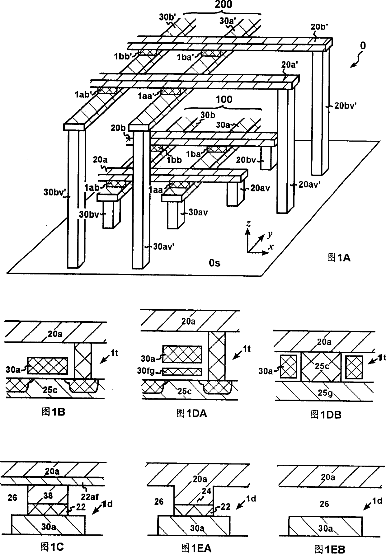
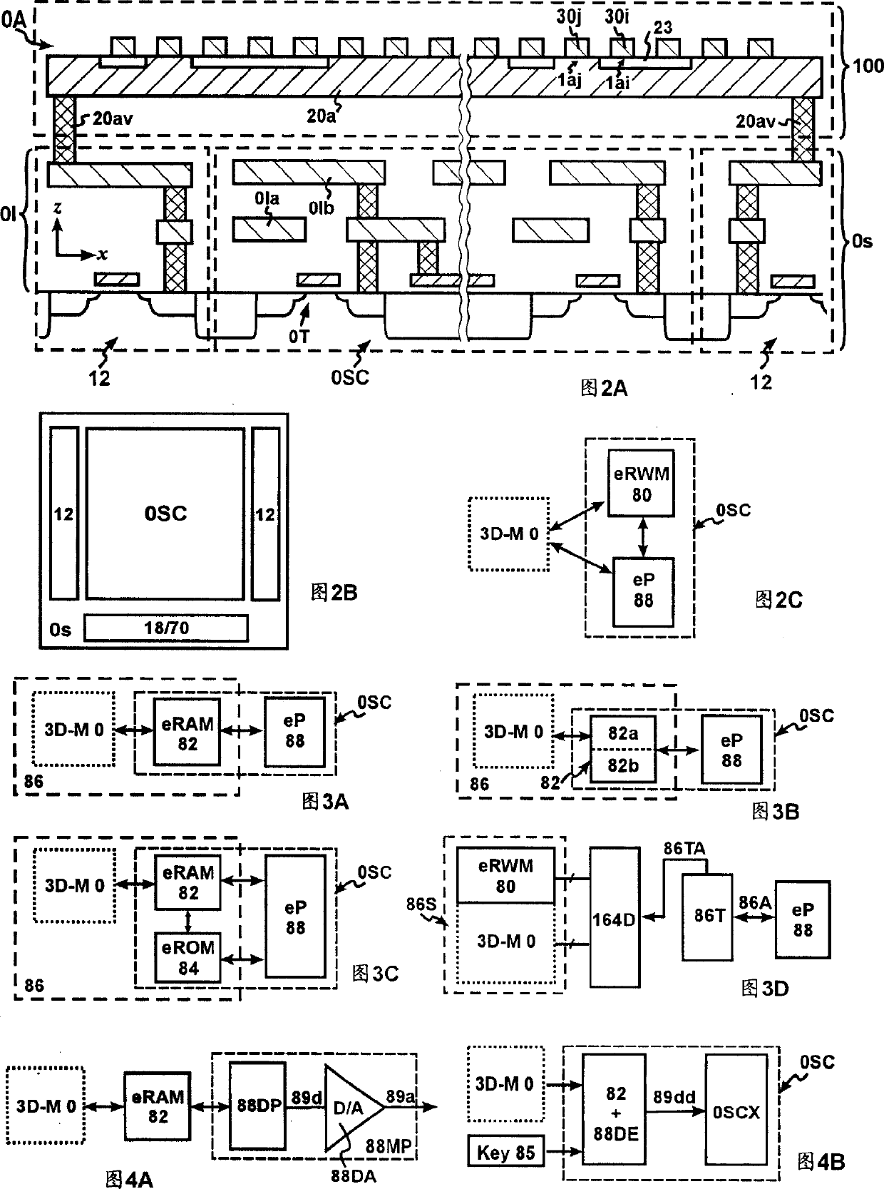
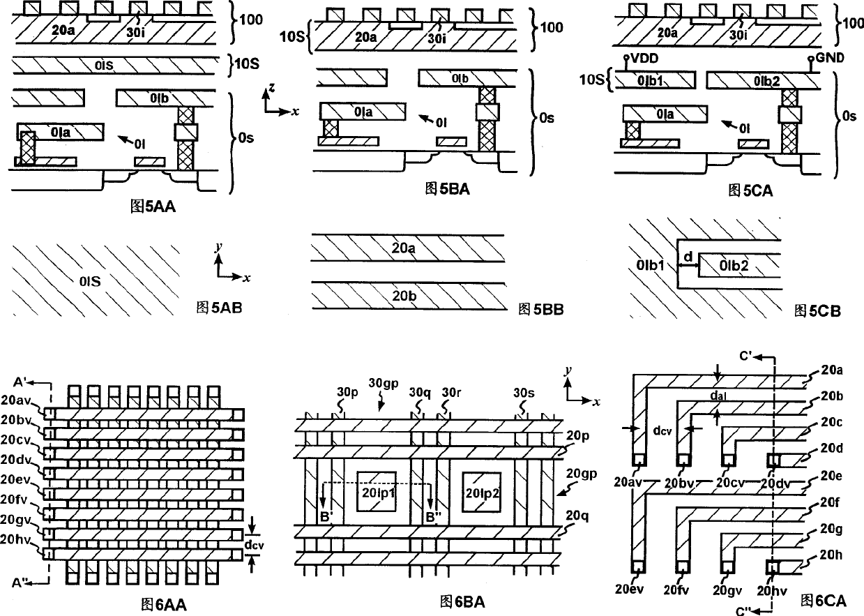
[0046] 1. Three-dimensional integrated memory-memory (3DiM)

[0047] FIG. 2A is a cross-sectional view of a three-dimensional integrated memory (3DiM). 3DiM integrates the 3D-M array 0A and the substrate circuit 0s. The 3D-M array OA includes one or more three-dimensional storage layers 100 . Each three-dimensional storage layer 100 contains multiple address selection lines (20a, 30i...) and multiple 3D-M cells (1ai...). These address select lines contain metallic material and / or doped semiconductor material. The transistor 0T on the substrate and its interconnection 0I (0Ia, 0Ib...) constitute the substrate circuit 0s. From a circuit point of view, the substrate circuit OS includes a substrate integrated circuit OSC and address decoders 12, 18 / 70 (FIG. 2B). These address decoders 12, 18 / 70 provide address decoding for the 3D-M array OA. Contact vias (20av...) provide electrical connections for address select lines (20a...) and substrate circuitry Os (eg address decoder)....


PUM


Abstract

A method based on electrically programmed 3D memory (EP-3DM) for the self-test of IC features that as said EP-3DM is suitable for storing the test data of an IC to be tested (CUT) in it, the IC containing said CUT and EP-3DM can support self-test. Its advantages are less influence of EP-3DM to the profile of CUT and broad bandwidth for supporting the homogeneous self-test.

Description

[0001] The present invention is a divisional application of the invention patent application with the application number 02131089.0, the application date is September 30, 2002, and the invention name is "three-dimensional integrated memory". technical field [0002] The present invention relates to the field of integrated circuits, more specifically, to electrically programmed three-dimensional integrated memories. Background technique [0003] In a three-dimensional integrated circuit (abbreviated as 3D-IC), one or more three-dimensional integrated circuit layers (abbreviated as 3D-IC layers) are stacked on a substrate in a direction perpendicular to the substrate. The 3D-IC layer is composed of non-single crystal (ie, polycrystalline or amorphous) semiconductor materials, which can have functions such as logic, storage, and simulation. For 3D-IC layers with logic and analog functions, they are more sensitive to defects. Du...

Claims


Application Information

Patent Timeline
IPC IPC(8): G11C29/00H01L21/66H01L27/10H01L27/115
Inventor 张国飙
Owner 张国飙
Why Eureka
Try Eureka