Check patentability & draft patents in minutes with Patsnap Eureka AI!

Electrooptical device and electronic appliance

An electro-optic device and electrode technology, which is applied in the direction of electric light source, identification device, lighting device, etc., can solve the problems of difficulty in meeting, uneven display, and inability to form a sufficiently large storage capacitor.

Inactive Publication Date: 2004-05-26
SEIKO EPSON CORP
View PDF0 Cites 13 Cited by
  • Summary
  • Abstract
  • Description
  • Claims
  • Application Information

AI Technical Summary

Problems solved by technology

[0005] However, in conventional electro-optical devices, there is a problem that the above-mentioned storage capacitor cannot be formed sufficiently large.
If the storage capacitance cannot be formed sufficiently large, the electric field applied to the electro-optic material such as liquid crystal cannot be sufficiently maintained during the above-mentioned full selection period, and as a result, display unevenness will occur on the image. or flashing etc.
[0006] In order to cope with such a problem, it is ideal to increase the size of the storage capacitor, but today, as electro-optical devices are being miniaturized, refined, or have a higher aperture ratio, it is becoming difficult to meet this requirement.
For example, if it is desired to simply increase the storage capacity, it is conceivable to try to increase the area of ​​the upper electrode and the lower electrode constituting the storage capacitor. It is impossible to meet the fundamental requirements for an electro-optic device to display bright images
[0007] In addition, in order to increase the storage capacity, it is conceivable to narrow the distance between the upper electrode and the lower electrode, that is, to reduce the thickness of the dielectric film. However, even under the current situation, due to the The thickness has been thinned to a considerable extent, so such attempts have reached the limit

Method used


Image

  • Electrooptical device and electronic appliance
  • Electrooptical device and electronic appliance
  • Electrooptical device and electronic appliance

Examples


Embodiment Construction

[0080] Hereinafter, embodiments of the present invention will be described with reference to the drawings. The following embodiments are embodiments in which the electro-optical device of the present invention is applied to a liquid crystal device.

[0081] (Constitution of the pixel part)

[0082] First, see Figure 1 to Figure 4 The configuration of the pixel portion of the electro-optical device according to Embodiment 1 of the present invention will be described.

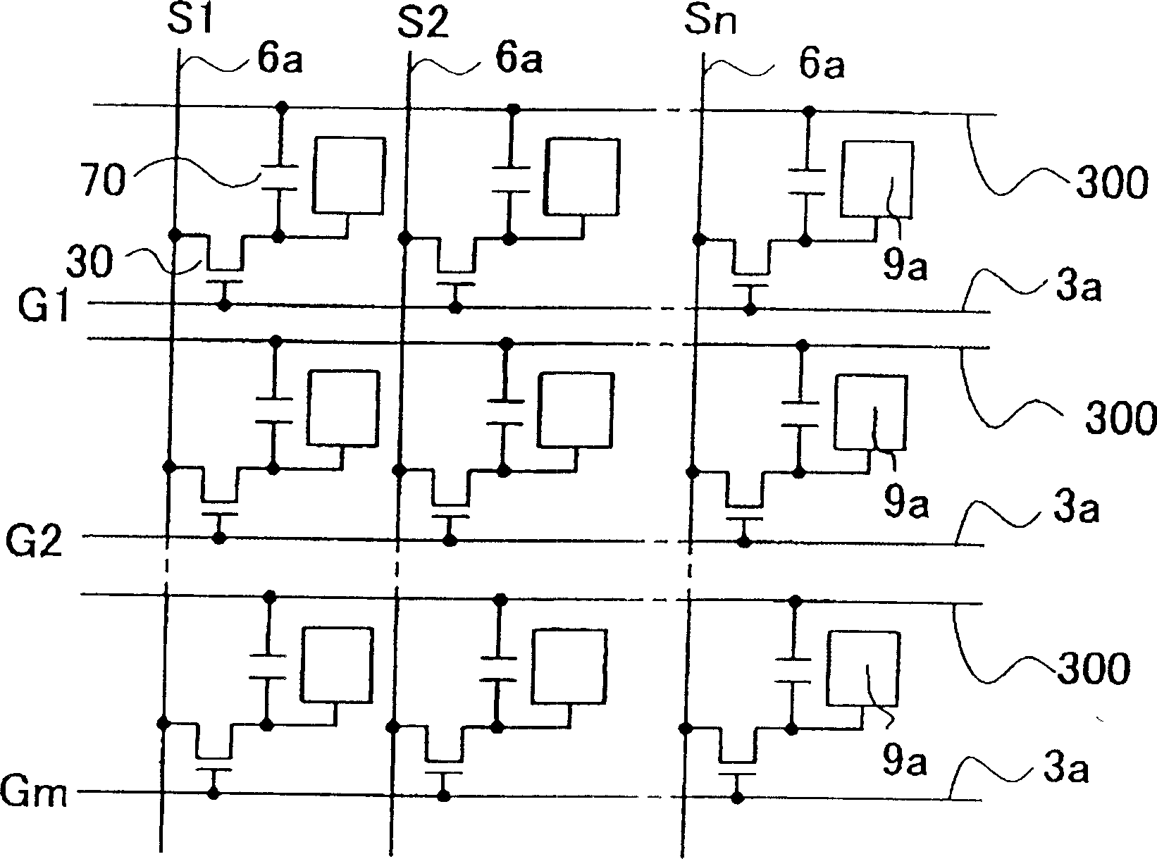
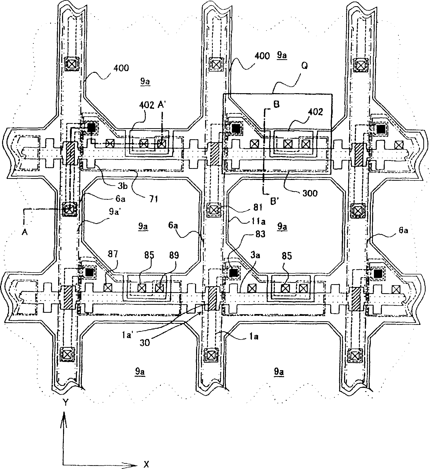
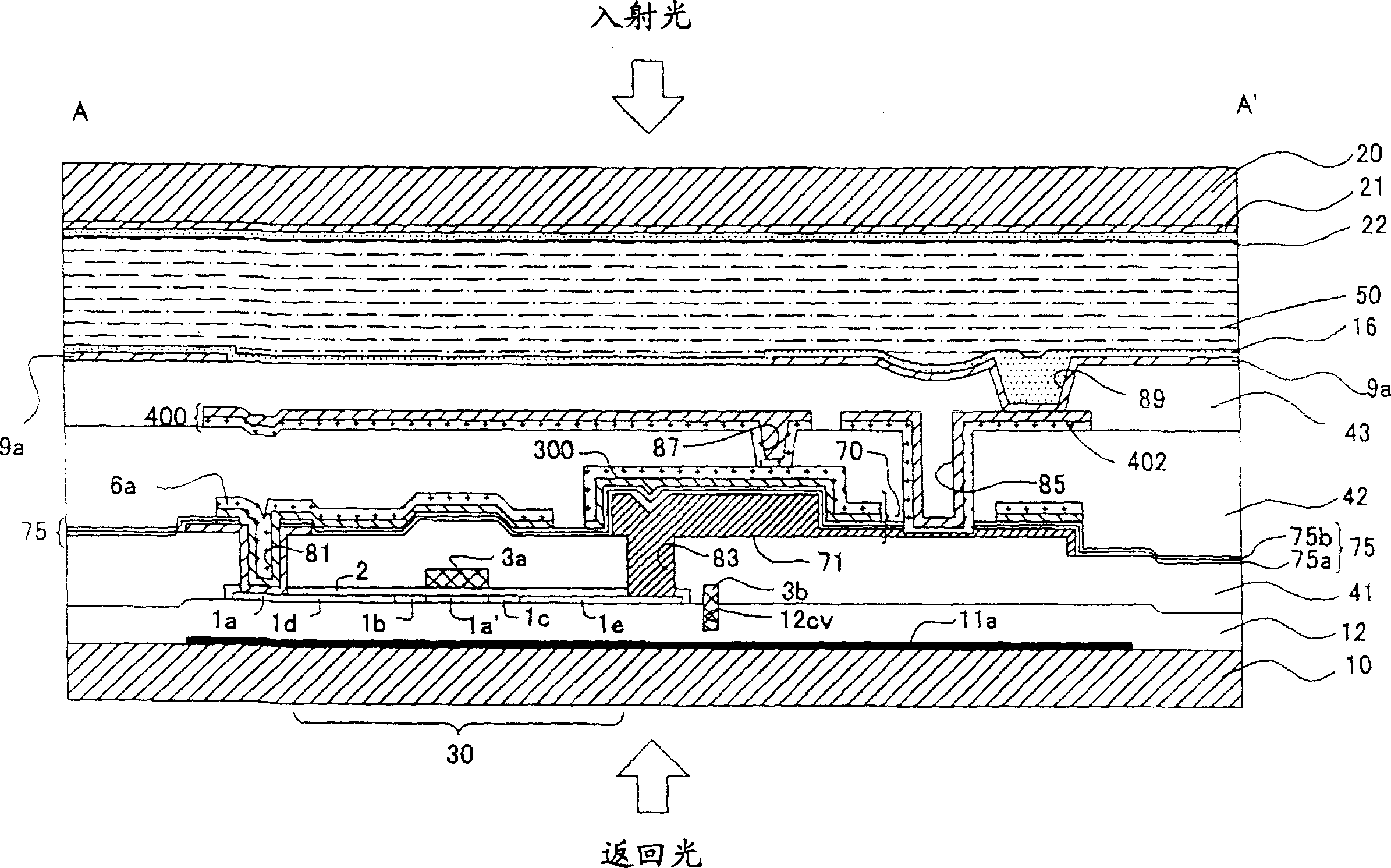
[0083] figure 1 is a circuit diagram showing an equivalent circuit of various elements, wiring, and the like provided on a plurality of pixels formed in a matrix forming an image display region of an electro-optical device. figure 2 It is a plan view of a plurality of adjacent pixel groups of a TFT array substrate on which data lines, scanning lines, pixel electrodes, etc. have been formed. image 3 yes figure 2 The A-A' profile, Figure 4 yes figure 2 The B-B' profile. In addition, in image 3 and ...


PUM

PropertyMeasurementUnit
heightaaaaaaaaaa
thicknessaaaaaaaaaa

Abstract

The present invention provides an electro-optical device and electronic apparatus. The electro-optical device includes, above a substrate, data lines extending in a first direction, scanning lines which extend in a second direction and which cross the data lines, pixel electrodes and thin film transistors disposed so as to correspond to regions in which the data lines and the scanning lines cross, storage capacitors electrically connected to the thin film transistors and the pixel electrodes, and a shield layer disposed between the data lines and the pixel electrodes. An upper electrode and a lower electrode between which a dielectric film forming each storage capacitor is supported including a first portion laminated along a plane parallel with one surface of the substrate and a second portion laminated along a plane orthogonal to the surface of the substrate, the sectional shape of the capacitor including a projecting shape.

Description

technical field [0001] The present invention belongs to the technical field of electro-optical devices and electronic equipment, and in particular, belongs to the technical field of electro-optical devices equipped with storage capacitors that improve the potential holding characteristics of pixel electrodes and electronic equipment configured to include the electro-optical devices. In addition, the present invention also belongs to the technical field of electrophoretic devices such as electronic paper or EL (electroluminescence) devices or devices using electron emission elements (field emission displays and surface conduction electron emission displays). Background technique [0002] It is known that thanks to having pixel electrodes arranged in a matrix and thin film transistors (hereinafter, appropriately referred to as 'TFT') connected to each of the pixel electrodes, connected to each of the TFTs, Scanning lines and data lines are arranged parallel to the row and colu...

Claims


Application Information

Patent Timeline
Patent Type & Authority Applications(China)
IPC IPC(8): G02F1/1333G02F1/133G02F1/1362G02F1/1368G02F1/167G09F9/30G09G3/06G09G3/30H01L29/04H05B33/00
CPCG02F1/136213G02F1/133
Inventor 壹岐拓则恒川吉文林朋彦
Owner SEIKO EPSON CORP
Features
  • R&D
  • Intellectual Property
  • Life Sciences
  • Materials
  • Tech Scout
  • Unparalleled Data Quality
  • Higher Quality Content
  • 60% Fewer Hallucinations
Learn More