CMOS transistor inverter with multiple grid transistor

An oxide semiconductor and transistor technology, which is applied in semiconductor devices, semiconductor/solid-state device manufacturing, transistors, etc., can solve the problems that the inverter circuit of multi-gate MOSFET has not been proposed yet, and is difficult to avoid short channel effect. , improve performance, good grid control effect

Inactive Publication Date: 2004-06-23
TAIWAN SEMICON MFG CO LTD
View PDF1 Cites 16 Cited by
  • Summary
  • Abstract
  • Description
  • Claims
  • Application Information

AI Technical Summary

Problems solved by technology

However, in terms of circuit optimization, an inverter circuit using only multi-gate MOSFETs has not been proposed so far.
But it is quite difficult to find a simple way to provide the best P / N width ratio for inverters with multi-gate MOSFETs

Method used


Image

  • CMOS transistor inverter with multiple grid transistor
  • CMOS transistor inverter with multiple grid transistor
  • CMOS transistor inverter with multiple grid transistor

Examples


Embodiment Construction

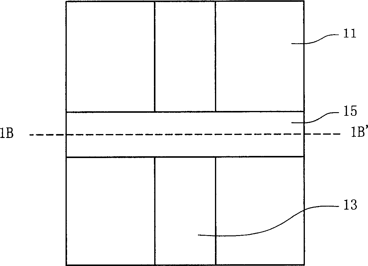
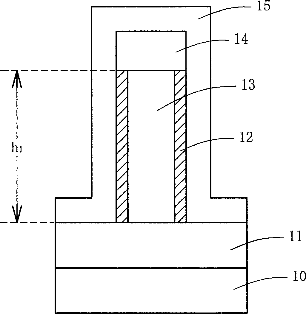
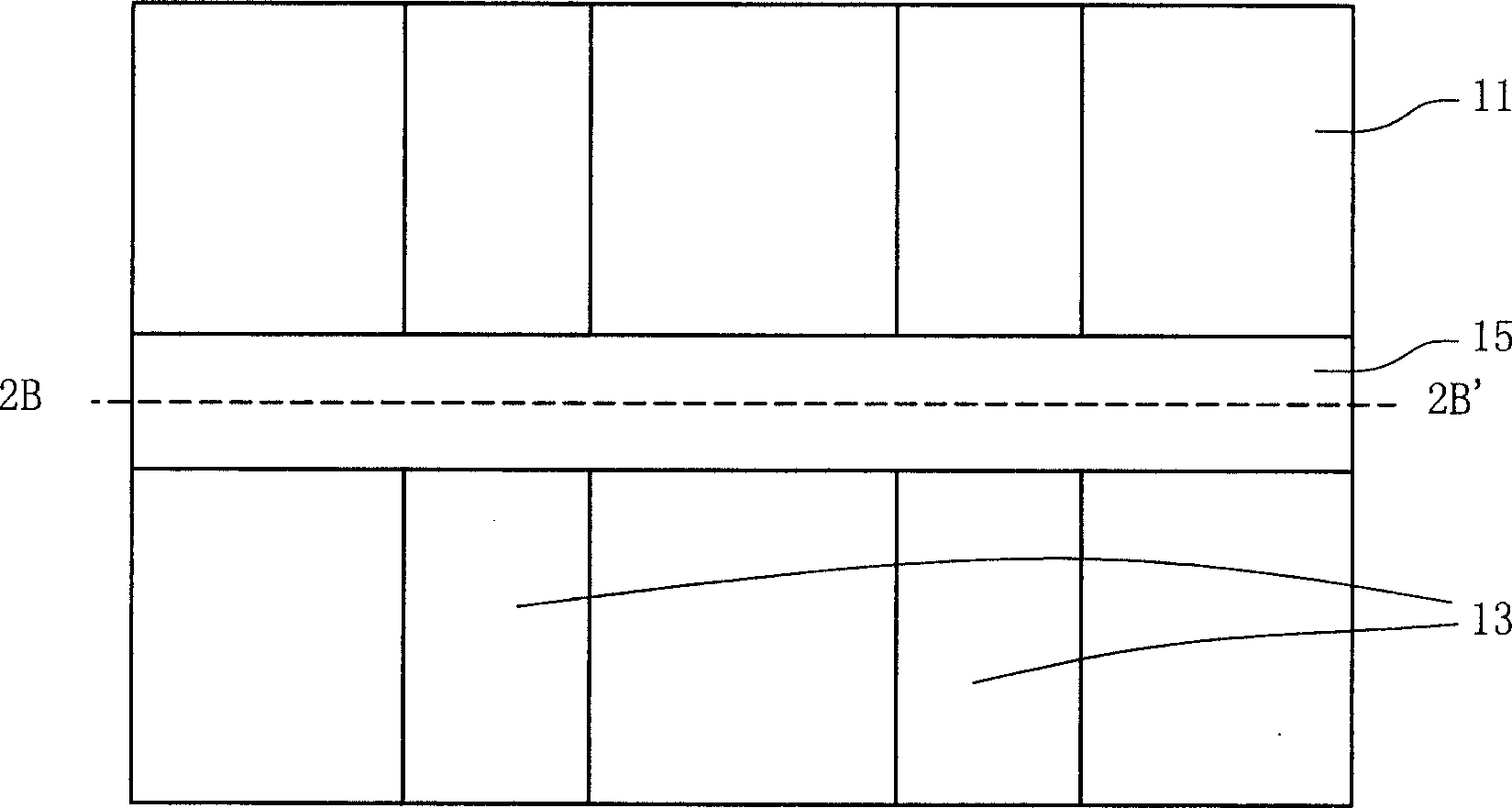
[0071] The present invention proposes a complementary metal-oxide-semiconductor transistor inverter using multi-gate MOSFETs.

[0072] In the present invention, an inverter circuit is configured using a multi-gate MOSFET having a gate on the top surface of a semiconductor fin to solve the existing problems. The multi-gate MOSFET with a gate on the top surface of the semiconductor fin includes a tri-gate MOSFET and an Omega field effect transistor (Ω-FET). A tri-gate MOSFET structure has three gates, one on the top surface of the semiconductor fin and two on either side of the semiconductor fin. Tri-gate assemblies have better gate control than dual-gate assemblies due to the addition of an additional gate on top of the semiconductor fin.

[0073] Figure 4A is the top view of the Tri-Gate MOSFET, Figure 4B for along Figure 4A Schematic diagram of the cross-sectional structure of 4B-4B′. A tri-gate MOSFET is very similar to a double-gate MOSFET, except that the etch mask...


PUM


Abstract

The CMOS transistor inverter includes at least one first multiple grid transistor, which includes one first source connected to the first power source, the first drain connected to the output end and the first grid; at least one second multiple grid transistor, which includes the second source connected to ground, the second drain connected to the output end and the second grid; and one input end contained to the first grid and the second grid.

Description

technical field [0001] The present invention relates to a silicon on insulator (SOI) circuit, and more particularly to a CMOS transistor inverter using a multi-gate transistor. Background technique [0002] Metal-oxide-semiconductor field effect transistor (MOSFET) technology is the most important semiconductor technology in the production of ultra-large scale integrated circuits (ultra-large scale integrated, ULSI). Over the past few years, reductions in the size of MOSFETs have provided continuous improvements in speed performance, circuit density, and cost per unit function. As the gate length of conventional MOSFETs becomes smaller and smaller, the interaction between the source and drain and the channel and gate will increase, thus affecting the channel potential. Therefore, a MOSFET with a short gate length has the problem that the gate cannot actually control the channel on and off. This weakening of MOSFET gate control is known as short-channel effects. Generally ...

Claims


Application Information

Patent Timeline
Patent Type & Authority Applications(China)
IPC IPC(8): H01L21/336H01L21/8238H01L27/092H01L27/12H01L29/786
CPCH01L29/785H01L27/092H01L21/845H01L21/823828H01L29/66795H01L29/7854H01L27/1211
Inventor 杨育佳杨富量胡正明
Owner TAIWAN SEMICON MFG CO LTD
Why Eureka
Try Eureka