Method for growing epitaxial chip of nitride LED structure by MOCVD

A technology of light-emitting diodes and epitaxial wafers, applied in gaseous chemical plating, coating, metal material coating process, etc., can solve problems such as the influence of GaN buffer layer LED structure performance

Inactive Publication Date: 2004-06-30
EPILIGHT TECH +1
View PDF0 Cites 33 Cited by
  • Summary
  • Abstract
  • Description
  • Claims
  • Application Information

AI Technical Summary

Problems solved by technology

Moreover, the selection of its change rate may also have an important impact on the quality of the GaN buffer layer and the performance of the LED structure on it.

Method used


Image

  • Method for growing epitaxial chip of nitride LED structure by MOCVD
  • Method for growing epitaxial chip of nitride LED structure by MOCVD
  • Method for growing epitaxial chip of nitride LED structure by MOCVD

Examples


Embodiment 1

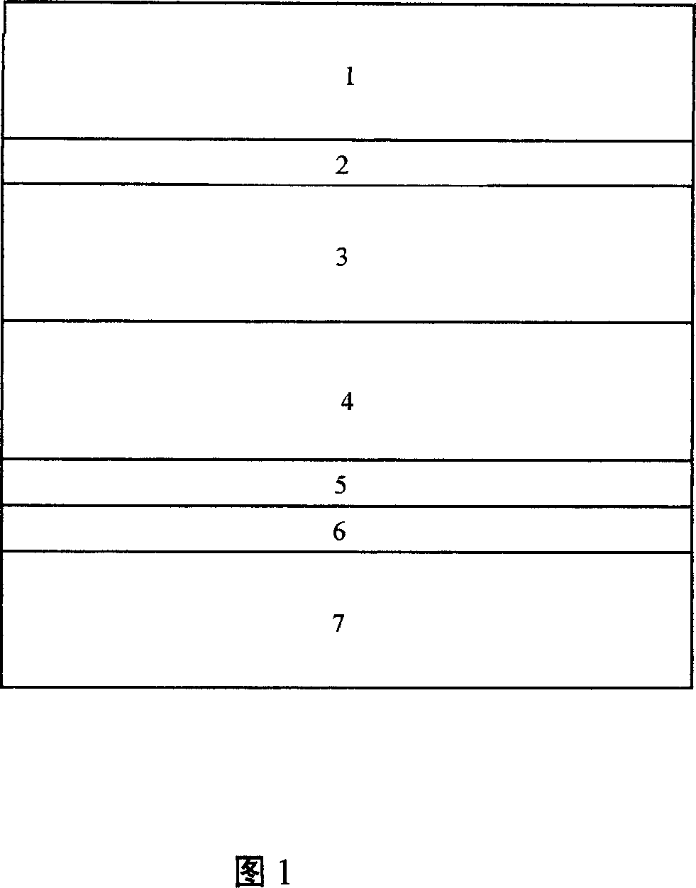
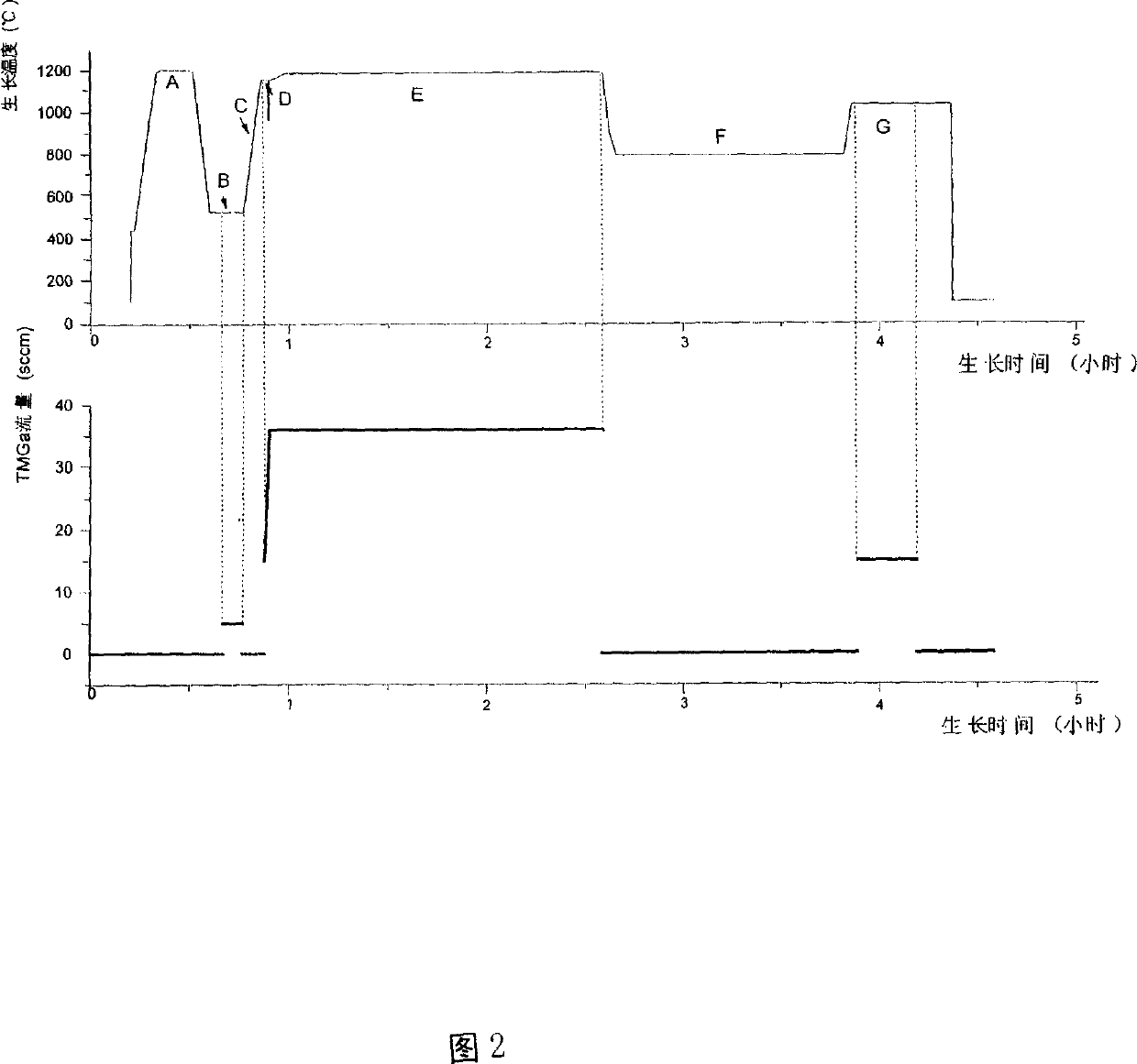
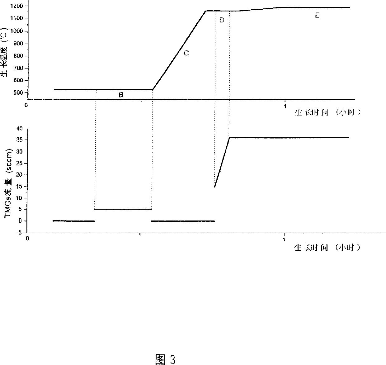
[0023] Using Aix 2000HT MOCVD system to epitaxially grow GaN-based ultra-high brightness LED structure epitaxial wafers. The substrate is (0001) sapphire (Al 2 o 3 ). As shown in Figure 1, first, the substrate 7 is heated to 1200°C, and treated at high temperature under hydrogen for 10 minutes; then the temperature is lowered to 500-540°C to grow a GaN nucleation layer 6, about 25 nanometers, and the flow rate of TMGa is 2.2×10 -5 mol / min, NH 3 The flow rate is 5 liters / minute; thereafter, the growth temperature is raised to 1160° C. to anneal the nucleation layer 6 for 4-8 minutes. After the annealing, at 1160° C., by linearly changing the flow rate of TMGa, the variable-rate epitaxial growth of the GaN buffer layer 5 was started, and the growth time was 90 seconds. TMGa flow from 2-6.63 to 15-20×10 -5 mol / min, NH 3 The flow rate is 3.5 l / min. Thereafter, the growth temperature was increased to 1180° C., and a GaN buffer layer with a thickness of 3.5 microns was grown ...

Embodiment 2

[0025] Using Aix 2000HT MOCVD system to epitaxially grow GaN-based ultra-high brightness LED structure epitaxial wafers. The substrate is (0001) sapphire (Al 2 o 3 ). As shown in Figure 1, first, the substrate 7 is heated to 1200°C, and treated at high temperature under hydrogen for 10 minutes; then the temperature is lowered to 510-540°C to grow a GaN nucleation layer 6, about 25 nanometers, and the flow rate of TMGa is 2.2×10 -5 mol / min, NH 3 The flow rate is 5 liters / minute; thereafter, the growth temperature is raised to 1160° C. to anneal the nucleation layer 6 for 4-8 minutes. After the annealing, at 1160° C., by linearly changing the flow rate of TMGa, the variable-rate epitaxial growth of the GaN buffer layer 5 was started, and the growth time was 90 seconds. TMGa from 2-6.63 to 15-17.7×10 -5 mol / min, NH 3 The flow rate is 3.5 l / min. Thereafter, the growth temperature was increased to 1180° C., and a GaN buffer layer with a thickness of 3.5 microns was grown at ...


PUM

PropertyMeasurementUnit
thicknessaaaaaaaaaa
thicknessaaaaaaaaaa
emission peakaaaaaaaaaa

Abstract

The invention relates to a method to use MOCVD to grow nitride LED structured epitaxial piece. First, heat the sapphire substrate to 1200 deg.C in MOCVD reaction room, and make high-temperature treatment under hydrogen, then reduce the temperature to 490-550 deg.C to grow GaN nucleating layer, then raise the growing temperature to 1100-1180 deg.C to anneal the nucleating layer, then under the final annealing temperature, start the epitaxial growth of GaN buffer layer at variable speed by linear change of TMGa flow, after this, grow a 2-4mum thick GaN buffer layer at a uniform speed, make the epitaxial growth of device structure on the 2-4mum thick GaN buffer layer and optimize the variable speed by growing InGaN / GaN multi-quantum trap LED structure on the 2-4mum thick GaN buffer layer. It can effectively realize the transition from 3-dimensional growth to 2-dimensional growth, improving the quality and luminous intensity of the epitaxial piece.

Description

technical field [0001] The invention relates to a GaN-based metal-organic vapor deposition (MOCVD) epitaxial growth method of III-V nitride materials, in particular to the growth of nitride multi-quantum well blue, green and purple light-emitting diode structure epitaxial wafers . Background technique [0002] GaN-based semiconductor materials have a band gap from 1.95 to 6.4eV, and their emission wavelengths almost cover the entire visible light region. Due to their huge application prospects, they have been extensively researched and developed. Especially the research, production and application of blue, green, violet and white diodes based on this new semiconductor material. At present, the most important, most effective and most extensive epitaxial growth of GaN-based semiconductor materials and devices is MOCVD technology. [0003] In the MOCVD growth nitride (GaN, AlN, InN and their alloys) technology, since there is no substrate material that matches the GaN lattice...

Claims


Application Information

Patent Timeline
Patent Type & Authority Applications(China)
IPC IPC(8): C23C16/34H01L21/205H01L21/365
Inventor 童玉珍张国义周建辉黎敏秦志新张昊翔丁晓民李树明
Owner EPILIGHT TECH
Why Eureka
Try Eureka