Method for growing photoelectric material and device through two-step method

A technology of optoelectronic materials and devices, which is applied in the direction of electrical components, semiconductor devices, metal material coating technology, etc., can solve the problems of crystal quality improvement and quality control, and achieve the reduction of XRD diffraction crystal surface half-width and photoelectric conversion efficiency The effect of improving and increasing production capacity

Pending Publication Date: 2015-05-27
西安利科光电科技有限公司
View PDF4 Cites 9 Cited by
  • Summary
  • Abstract
  • Description
  • Claims
  • Application Information

AI Technical Summary

Problems solved by technology

[0006] The present invention comprehensively utilizes magnetron sputtering technology and metal-organic chemical vapor deposition technology, conducts in-depth research and improvement on the problem that the quality of low-temperature nucleation is difficult to control and the crystal quality is difficult to improve in the current technology, and proposes a two-step method Methods of growing optoelectronic materials and devices

Method used


Image

  • Method for growing photoelectric material and device through two-step method
  • Method for growing photoelectric material and device through two-step method
  • Method for growing photoelectric material and device through two-step method

Examples


Embodiment 1

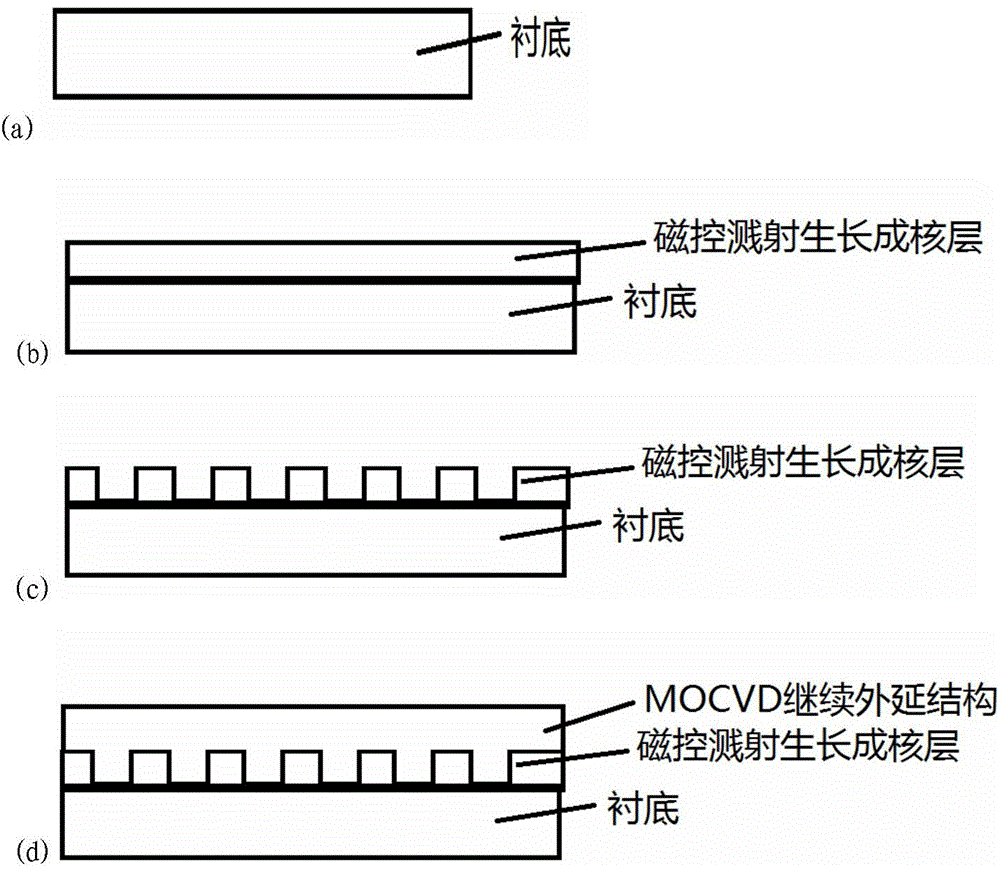
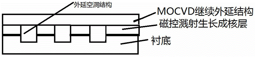
[0024] First, the existing sapphire PSS substrate material is used to deposit AlN material in the magnetron sputtering equipment, the deposition thickness is 25nm, and then the substrate material deposited with the AlN buffer layer is transferred to the MOCVD equipment for high temperature treatment, and the processing temperature is 1100 degrees. After the pressure is 200mbar and the processing time is 3min (the optimized result), the high temperature deposition of non-doped GaN, N-type doped GaN, stress release layer, multiple quantum well layer, electron blocking layer and P-type GaN structure LED is started. As a comparison, the same PSS substrate is directly epitaxially grown in MOCVD, first depositing AlN with a thickness of 25nm, then 1100 degrees, pressure 200mbar, and after 3 minutes of processing time, high-temperature deposition of non-doped GaN, N-type doped GaN, stress release layer, multi-quantum well layer, electron blocking layer and P-type GaN structure LED. A...

Embodiment 2

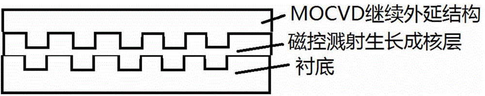
[0026] Use the existing sapphire PSS substrate material to deposit AlN material in the magnetron sputtering equipment, the deposition thickness is 15nm, and then pattern the PSS substrate material deposited with the AlN buffer layer as figure 2 The structure shown in the figure is then transferred to MOCVD equipment for high-temperature treatment. The treatment temperature is 1100 degrees, the pressure is 200mbar, and the treatment time is 2.5 minutes (optimized results). After that, high-temperature deposition of non-doped GaN, N-type doped GaN, and stress release layer begins , multi-quantum well layer, electron blocking layer and P-type GaN structure LED. For comparison, on the same PSS sapphire substrate, epitaxial growth is directly carried out in MOCVD. First, AlN is deposited with a thickness of 15nm, and then 1100 degrees, a pressure of 200mbar, and a treatment time of 2.5 minutes. GaN, stress release layer, multi-quantum well layer, electron blocking layer and P-type...

Embodiment 3

[0028] Use the existing sapphire planar substrate material to deposit AlN material in the magnetron sputtering equipment, the deposition thickness is 25nm, and then pattern the substrate material deposited with the AlN buffer layer as follows: image 3The structure shown in the figure is then transferred to MOCVD equipment for high-temperature treatment. The treatment temperature is 1100 degrees, the pressure is 200mbar, and the treatment time is 3 minutes (optimized results). After that, high-temperature deposition of non-doped GaN, N-type doped GaN, and stress release layer, Multi-quantum well layer, electron blocking layer and LED with P-type GaN structure. As a comparison, epitaxial growth is directly carried out in MOCVD on the same sapphire flat substrate. First, AlN is deposited with a thickness of 25nm, and then 1100 degrees, a pressure of 200mbar, and a high temperature deposition of non-doped GaN and N-type doped GaN. , stress release layer, multi-quantum well layer,...


PUM

PropertyMeasurementUnit
thicknessaaaaaaaaaa
thicknessaaaaaaaaaa

Abstract

The invention comprehensively utilizes a magnetron sputtering technology and a metal organic chemical vapor deposition technology, conducts in-depth research and modification directed towards the problems that the quality of low-temperature nucleus formation is relatively difficult to control, and the quality of a crystal is difficult to promote, and provides a method for growing a photoelectric material and device through a two-step method. The method firstly adopts a material as a nucleus formation layer for follow-up growth, wherein the epitaxy of the material conducted magnetron sputtering on a substrate and the substrate material are different, the crystal grating mismatch degree of the epitaxy of the material with a follow-up epitaxy material is smaller than 10%, the material is polycrystalline or amorphous, and the thickness of the material is 1 nm to 10 [Mu]m; then the substrate growing the nucleus formation layer is sent to MOCVD equipment, wherein the temperature is 700-1,250 DEG C, and the pressure is 0-1,040 mbar; follow-up growth of a device structure is conducted after high temperature processing.

Description

Technical field: [0001] The invention relates to a method of growing photoelectric materials and devices. Background technique: [0002] The growth of existing optoelectronic materials and devices mainly includes: Molecular Beam Epitaxy (abbreviated as MBE), Metal Organic Chemical Vapor Deposition (abbreviated as MOCVD) and magnetron sputtering (Magnetron Sputtering) for epitaxy Growth of materials and devices. Among them, molecular beam epitaxy requires harsh conditions, requires extremely high vacuum, and the cost of substrate materials and growth is extremely high. It is generally used in special technical fields, and the control of equipment and the development of materials are still in the research and development stage and cannot be used as a stable quantity. Production; metal-organic chemical vapor deposition has been mass-produced and widely used in the mass production of various optoelectronic devices. The manufacturing cost is low and the process is controllable. ...

Claims


Application Information

Patent Timeline
Patent Type & Authority Applications(China)
IPC IPC(8): H01L33/00H01L33/32C23C14/34
CPCH01L33/32C23C14/35C23C16/44C23C16/52H01L33/0075
Inventor 李淼黄宏嘉
Owner 西安利科光电科技有限公司
Why Eureka
Try Eureka