Semiconductor storage

A memory and semiconductor technology, applied in the direction of semiconductor devices, static memory, digital memory information, etc., to achieve the effects of preventing damage, low current consumption, and preventing misoperation

Inactive Publication Date: 2004-07-28
SOCIONEXT INC
View PDF1 Cites 10 Cited by
  • Summary
  • Abstract
  • Description
  • Claims
  • Application Information

AI Technical Summary

Problems solved by technology

[0013] But when Figure 8 In the conventional semiconductor memory shown in , for example, when the bit line pair BITO, NBITO is selected, and for example, when the word line WLn is selected, in the selected memory cell 1A, the transfer transistors MN1A, MN2A Turn on, use the source potential control signal SLn to make the sources of the driving transistors MN3A and MN4A into a floating state, and transmit the potential difference of the bit lines BITO and NBITO to the memory cell 1A to write data, but even in the same row In the non-selected memory cell 1C, since the transfer transistors MN1C and MN2C are also turned on, and the sources of the drive transistors MN3C and MN4C are also in a floating state, the data stored at the storage nodes DC and NDC of the non-selected memory cell 1C are also turned on. Possibility of being overwritten
Therefore, a plurality of memory cells 1A, 1C connected to the same word line (for example, WLn) cannot be selected by the column selectors 3A, 3B.

Method used


Image

  • Semiconductor storage
  • Semiconductor storage
  • Semiconductor storage

Examples


no. 1 Embodiment

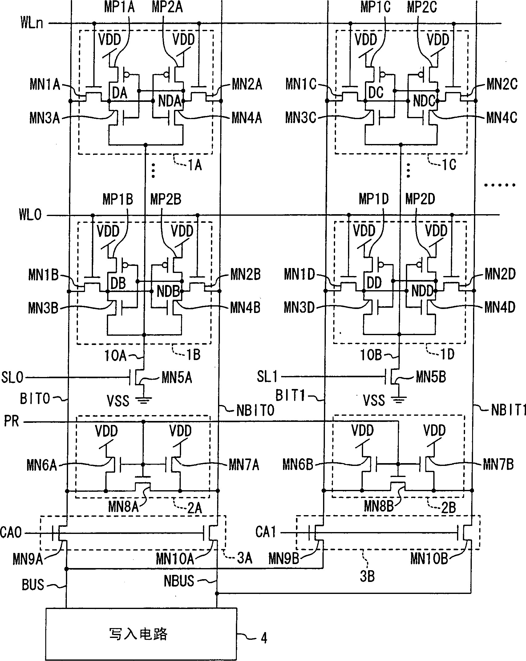
[0041] figure 1 A configuration diagram of a semiconductor memory device according to a first embodiment of the present invention is shown.

[0042] In this figure, a plurality of memory cells 1A to 1D are arranged in an array. The memory cell 1A will be described below as a representative. Since the other memory cells 1B to 1D have the same internal structure, they are attached with reference numerals B, C, and D, respectively, and their descriptions are omitted.

[0043] The memory cell 1A is composed of two P-type load transistors MP1A and MP2A, two N-type transfer transistors MN1A and MN2A, and two N-type drive transistors MN3A and MN4A. The sources of the two load transistors MP1A and MP2A are connected to the high-voltage power supply VDD and supplied with a high potential (first potential), and the drains are connected to the sources of the two transfer transistors MN1A and MN2A and the two drive On the drains of transistors MN3A and MN4A. The gates of the two load...

no. 2 Embodiment

[0056] Next, a semiconductor memory device according to a second embodiment of the present invention will be described.

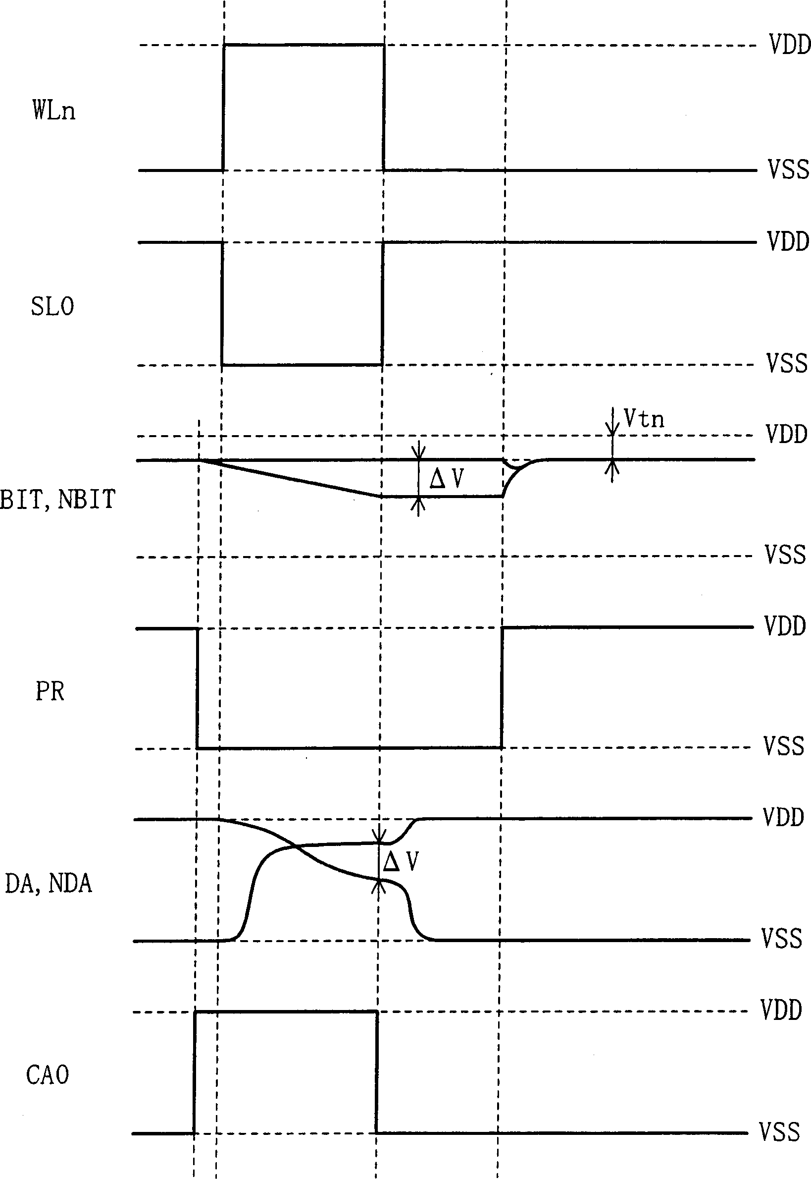
[0057] exist image 3 The semiconductor memory of this embodiment is shown in . In this figure, with figure 1 Compared with semiconductor memory, it is only different in the following aspects. That is, the balance transistors of the precharge and balance circuits 2A and 2B are composed of P-type transistors MP5A and MP5B, and the inverted signal of the precharge signal PR is input to the gates of these transistors.

[0058]In this embodiment, even if the potentials of the bit lines BITO, NBITO, BIT1, and NBIT1 are higher than the precharge potential VDD-Vtn, since the write circuit 4 is used to write data to the selected bit line (such as BITO, NBITO) The potential of one of the storage nodes DA and NDA in the memory cell 1A is pulled down to the ground potential VSS, and the data of the bit lines BITO and NBITO are transmitted to the memory cell 1A. Th...

no. 3 Embodiment

[0061] Next, a semiconductor memory device according to a third embodiment of the present invention will be described.

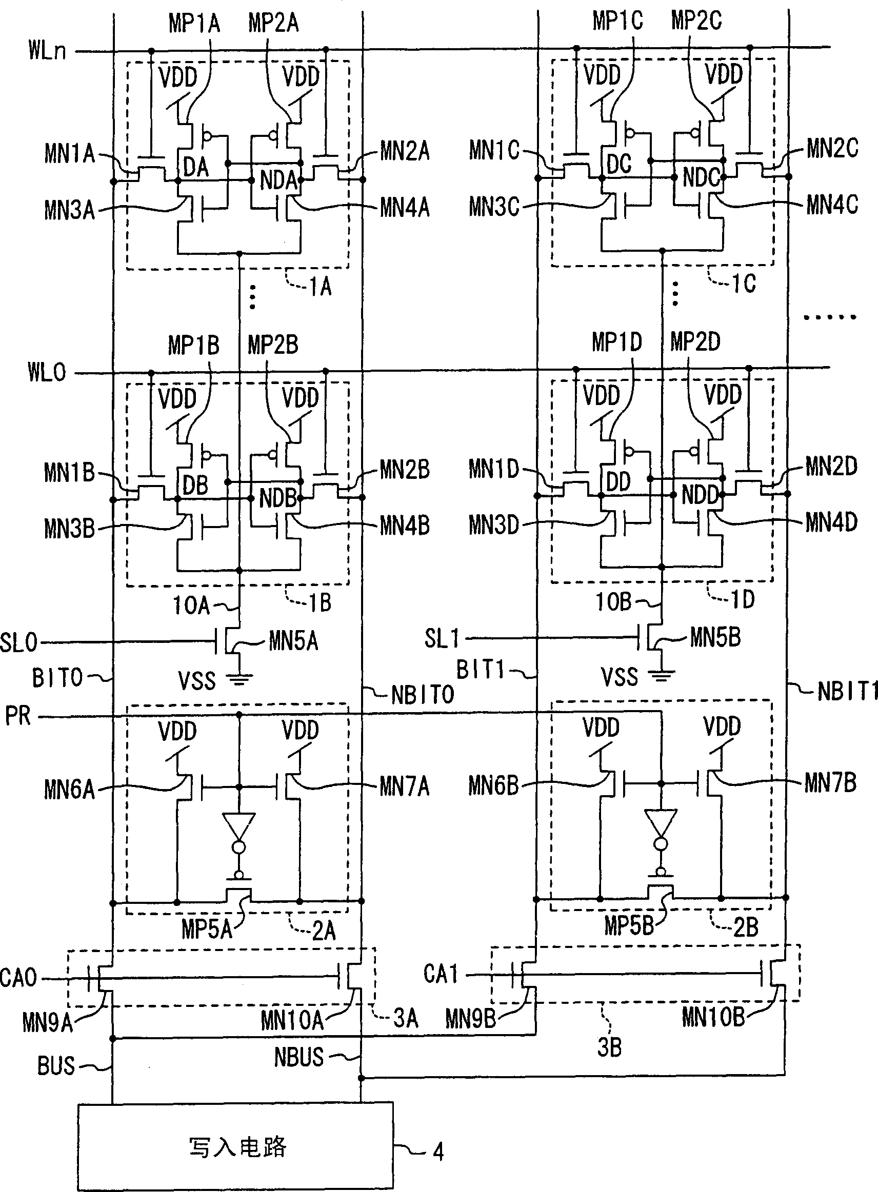
[0062] Figure 4 The semiconductor memory of this embodiment is shown in . The figure of semiconductor memory with figure 1 The semiconductor memory device of the first embodiment shown in FIG. 10 differs only in the following structure.

[0063] That is, in each of the memory cells 1A to 1D, the transfer transistors are composed of P-type transistors (MP3A and MP4A), (MP3B and MP4B), (MP3C and MP4C), (MP3D and MP4D), and word Inversion signal of line selection signals WLn to WL0. In addition, in the precharge and balance circuits 2A and 2B, the precharge transistors are composed of P-type transistors (MP5A and MP6A), (MP5B and MP6B), and the balance transistors are also composed of P-type transistors MP7A and MP7B. The inverted signal of the precharge signal PR is input to the pole. Furthermore, the column selectors 3A and 3B are respectively composed...


PUM


Abstract

The respective sources of drive transistors included in memory cells that are located in each of multiple columns and connected to a corresponding one of bit line pairs are connected commonly to a low voltage power supply VSS via an assertion transistor. When data is written, the assertion transistor for the memory cells connected to a selected one of the bit line pairs and located in the identical column is negated, so that the sources of the drive transistors in the memory cells in that column are allowed to float. Consequently, even with a low power supply voltage, it is possible to write the data into a single selected memory cell, while data in the unselected memory cells can be retained favorably.

Description

technical field [0001] The present invention relates to lower voltage and lower power consumption of semiconductor memories. Background technique [0002] Image 6 A conventional SRAM circuit is shown. This SRAM has a plurality of memory cells 1A to 1D arranged in an array. Since these memory cells have the same structure, the memory cell 1A will be described as an example. The memory cell 1A is composed of two load transistors MP1A, MP2A, two transfer transistors MN1A, MN2A, and two drive transistors MN3A, MN4A. The gates of the two transfer transistors MN1A, MN2A are connected to the word line WLn, and the drains are connected to the bit lines BITO, NBITO. The sources of the two load transistors MP1A and MP2A are connected to the high-voltage power supply VDD, and the sources of the two drive transistors MN3A and MN4A are connected to the low-voltage power supply VSS. Two latch circuits are formed by the load transistors MP1A, MP2A and the drive transistors MN3A, MN4A,...

Claims


Application Information

Patent Timeline
Patent Type & Authority Applications(China)
IPC IPC(8): G11C11/41G11C11/00G11C11/417G11C11/419H01L27/11
CPCG11C11/419
Inventor 金原旭成奥山博昭
Owner SOCIONEXT INC
Why Eureka
Try Eureka