Luminous device with dependent voltage/resistance layer

A technology of light-emitting elements and resistors, which is applied to electric solid-state devices, semiconductor/solid-state device components, electrical components, etc., can solve the problems of increasing the steps of connecting the light-emitting diode chip and the shunt diode, and increasing the cost, so as to avoid the complexity of the process. , the effect of reducing strict requirements and relaxing strict requirements

Inactive Publication Date: 2004-08-04
EPISTAR CORP
View PDF1 Cites 13 Cited by
  • Summary
  • Abstract
  • Description
  • Claims
  • Application Information

AI Technical Summary

Problems solved by technology

However, this invention connects the chip after cutting with the shunt diode, so the electrostatic damage in the LED chip process is still unavoidable. In addition, this process increases the steps of connecting the LED chip and the shunt diode, and the cost is relatively increased.

Method used


Image

  • Luminous device with dependent voltage/resistance layer
  • Luminous device with dependent voltage/resistance layer
  • Luminous device with dependent voltage/resistance layer

Examples


Embodiment Construction

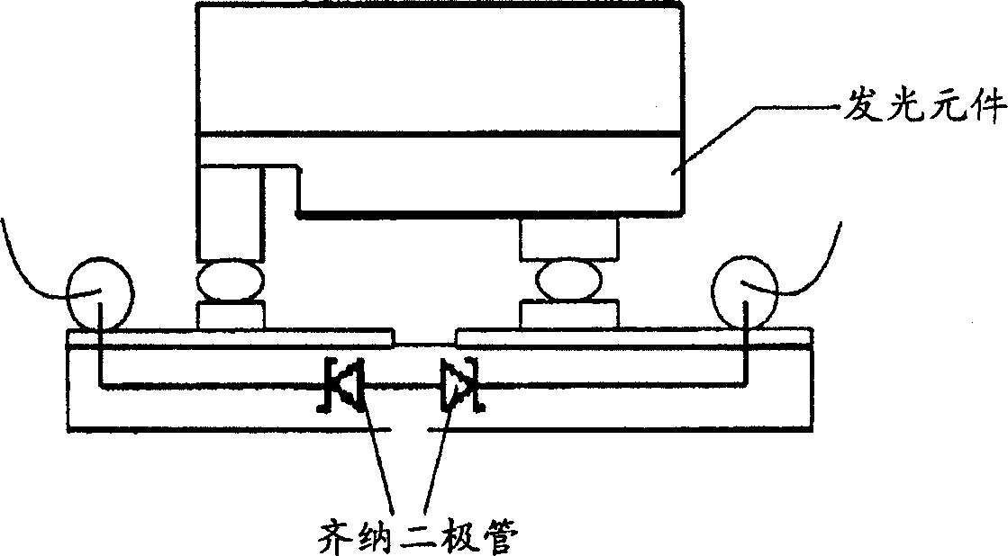
[0056] see Figure 5 According to a preferred embodiment of the present invention, a light-emitting element 1 with a voltage / resistance dependent layer includes a substrate 10; a light-emitting stack formed on the substrate 10, wherein the light-emitting stack includes a layer formed on the substrate 10 A first contact layer 11, wherein the first contact layer respectively includes a first surface region and a second surface region, a first confinement layer 12 formed on the first surface region, a first confinement layer 12 formed on the first confinement A light-emitting layer 13 on the layer 12, a second confinement layer 14 formed on the light-emitting layer 13, a second contact layer 15 formed on the second confinement layer 14; A first contact electrode 16; a second wiring electrode 17 formed on the second contact layer 15; Voltage / resistance dependent layer 18 .

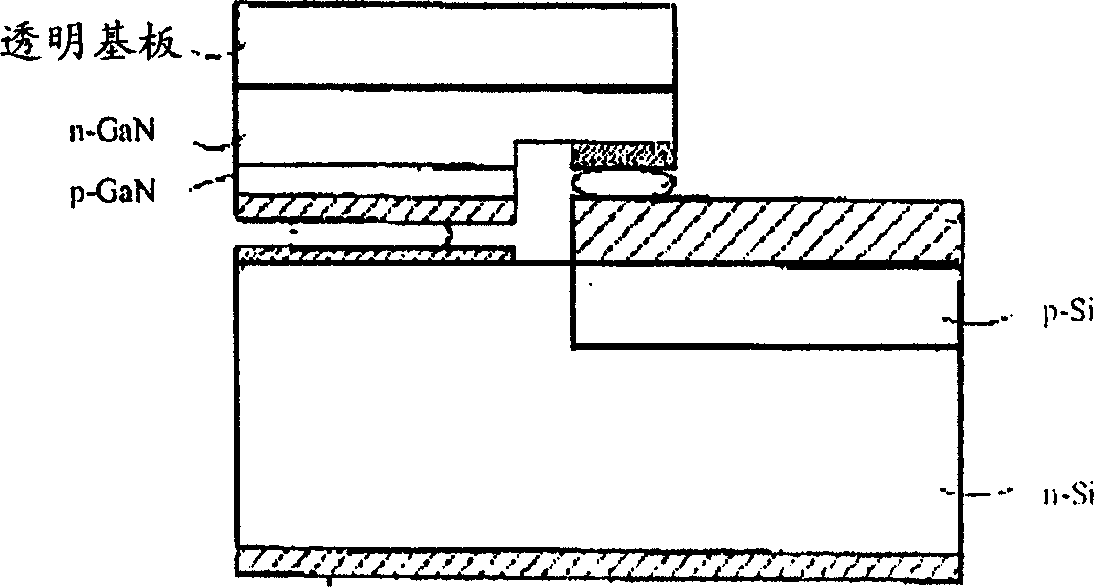
[0057] see Figure 6According to another preferred embodiment of the present invention, a light-emitting...


PUM


Abstract

A luminous device with dependent votlage/resistor layer is composed of a luminous unit with a first and second surfaces, the first electrode on the first surface, the secone electrode on the second surface, and a dependent voltage/resistor layer connected to both the first electrode and the second electrode for antistatic purpose.

Description

technical field [0001] The invention relates to a light-emitting element, in particular to a light-emitting element with a voltage / resistance dependent layer. Background technique [0002] Light emitting devices are widely used, for example, in optical display devices, laser diodes, traffic signs, data storage devices, communication devices, lighting devices, and medical devices. In this field, one of the important tasks for technicians at present is how to avoid damage to light-emitting elements caused by static electricity, so as to improve the pass rate of light-emitting elements. [0003] Such as figure 1 As shown, in order to avoid damage to the light-emitting element caused by static electricity in the light-emitting element of the prior art, a set of Zener diodes (Zener Diode) will be added when the light-emitting element is packaged, so that the electrostatic discharge caused by the environment can pass through the Zener diode In order to avoid damage to the light-...

Claims


Application Information

Patent Timeline
Patent Type & Authority Applications(China)
IPC IPC(8): H01L23/60H01L33/00
CPCH01L2224/16145
Inventor 刘文煌刘柏均谢明勋曾子峰欧震
Owner EPISTAR CORP
Why Eureka
Try Eureka