Plasma generation system

A plasma and generation system technology, applied in plasma, semiconductor/solid-state device manufacturing, discharge tube, etc., can solve the problem that plasma cannot be formed uniformly

Inactive Publication Date: 2004-08-04
SAMSUNG ELECTRONICS CO LTD
View PDF1 Cites 5 Cited by
  • Summary
  • Abstract
  • Description
  • Claims
  • Application Information

AI Technical Summary

Problems solved by technology

However, the microwaves passing through the waveguide diverge, so when the substrate is large, the plasma cannot be formed uniformly

Method used


Image

  • Plasma generation system
  • Plasma generation system

Examples


Embodiment Construction

[0021] Hereinafter, a preferred embodiment of the present invention will be described in detail with reference to the accompanying drawings.

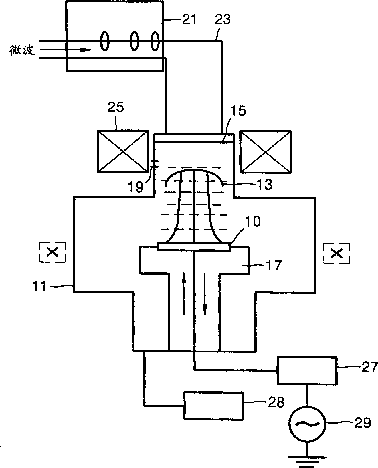
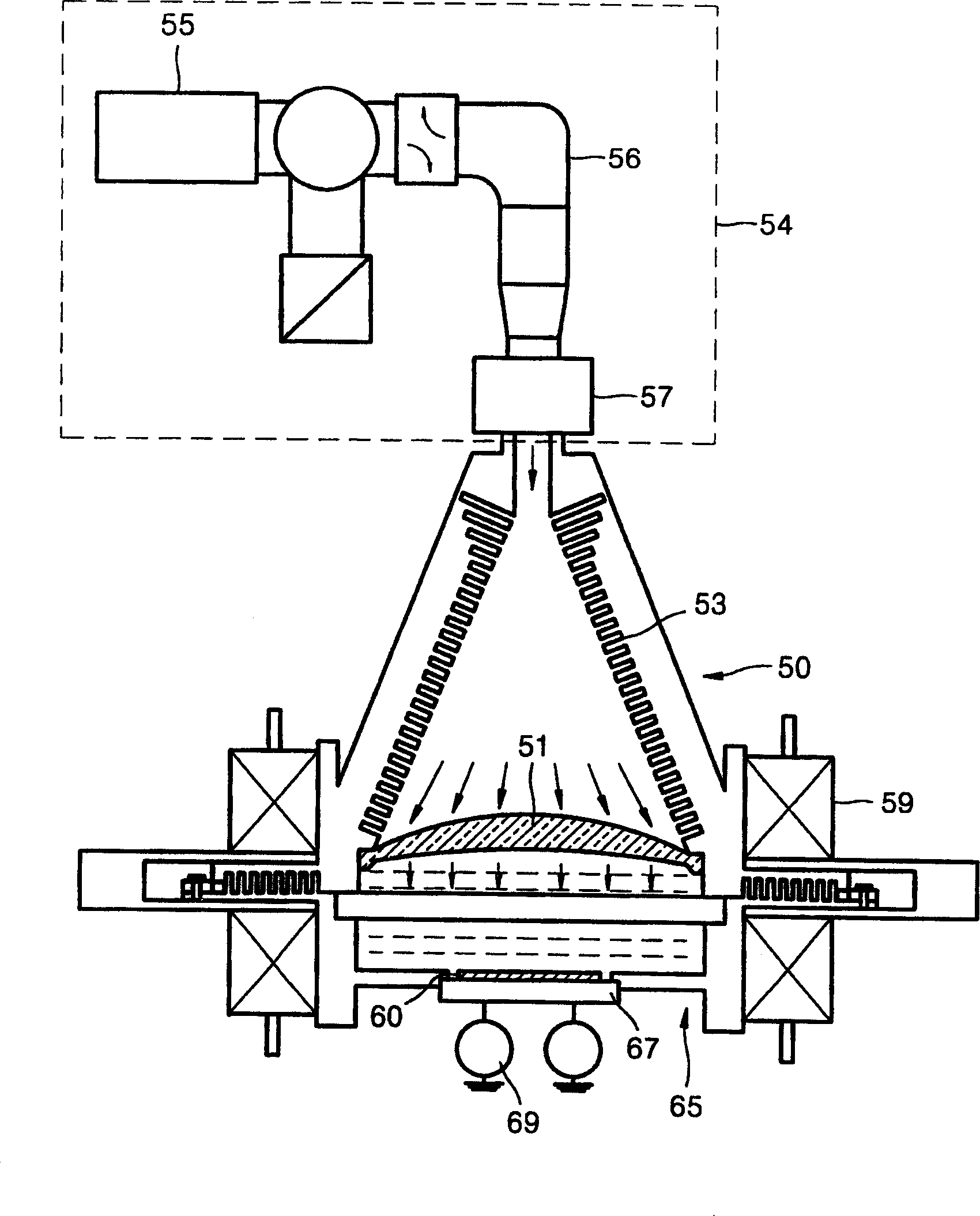
[0022] figure 2 The structure of the plasma generating system according to the embodiment of the present invention is schematically shown. refer to figure 2 A plasma generating system according to an embodiment of the present invention includes a microwave generator 54, a microwave conversion chamber 50 and a vacuum chamber 65 in which plasma etching is performed.

[0023] Microwave generator 54 comprises: a radio frequency energy source 55, is used to produce the ultra-high frequency microwave in the range of 300MHz to 1GHz; A waveguide 56, carries out microwave propagation through it; The microwaves are polarized in a single direction.

[0024] The microwave conversion chamber 50 is trumpet-shaped, and its width gradually increases in the direction of microwave propagation, so as to perform plasma etching on large-sized substrate...


PUM


Abstract

A plasma generation system that is capable of generating uniform high-density plasma includes a microwave generator for generating microwaves, a refractor for altering a direction of propagation of the microwaves, and an electromagnetic unit for applying a magnetic field to plasma formed by the microwaves to generate electron cyclotron resonance.

Description

technical field [0001] The invention relates to a plasma generation system, in particular to a plasma generation system capable of generating uniform high-density plasma. Background technique [0002] figure 1 The structure of a conventional electron cyclotron resonance (ECR) plasma device is schematically shown. [0003] refer to figure 1 A shower disk 13 is installed in the upper part of the processing chamber 11 , and gas for forming plasma is sent into the processing chamber 11 above the substrate 10 through the shower disk 13 . The substrate 10 is placed on the substrate holder 17 , and the RF bias generated by the RF energy source 29 in the range of 100 kHz to 15 MHz is applied to the substrate holder 17 through an adapter network 27 . [0004] An etching gas is supplied into the processing chamber 11 through the gas inlet 19 . The ultra-high frequency electromagnetic wave with a frequency of 300 MHz to 1 GHz generated by the radio frequency energy source 29 is con...

Claims


Application Information

Patent Timeline
Patent Type & Authority Applications(China)
IPC IPC(8): H05H1/18H01J37/32H01L21/3065H05H1/46
CPCH01J37/32266H01J37/32678H05H1/46H01J37/32192H05H1/18
Inventor 安德烈·佩特林许智贤申在光
Owner SAMSUNG ELECTRONICS CO LTD
Why Eureka
Try Eureka