Plasma processing device with very-high frequency parallel resonance antenna

A plasma and processing equipment technology, applied in the field of plasma processing equipment, can solve problems such as inability to generate resonance

Inactive Publication Date: 2003-01-22
JUSUNG ENG
View PDF0 Cites 33 Cited by
  • Summary
  • Abstract
  • Description
  • Claims
  • Application Information

AI Technical Summary

Problems solved by technology

However, products made of conventional variable capacitors used as the resonance capacitor C3 have a capacitance of 5pF or more, so the desired resonance in the RF region of 20MHz to 300MHz cannot be actually produced.

Method used


Image

  • Plasma processing device with very-high frequency parallel resonance antenna
  • Plasma processing device with very-high frequency parallel resonance antenna
  • Plasma processing device with very-high frequency parallel resonance antenna

Examples


Embodiment Construction

[0024] Detailed description of the preferred embodiment

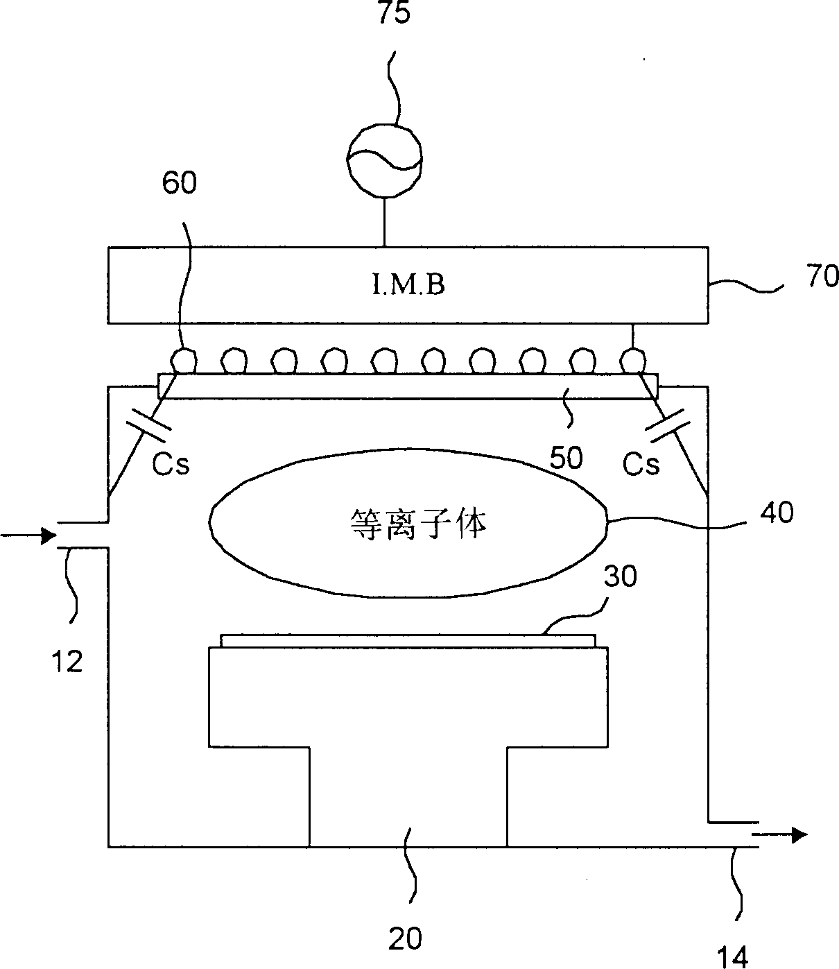
[0025] Now, preferred embodiments of the present invention will be described in detail with reference to the accompanying drawings. Regarding the reference numerals assigned to elements in the respective drawings, it should be noted that the same numerals as those assigned to elements in the conventional art represent elements performing the same functions, and thus their repeated descriptions are intentionally omitted.

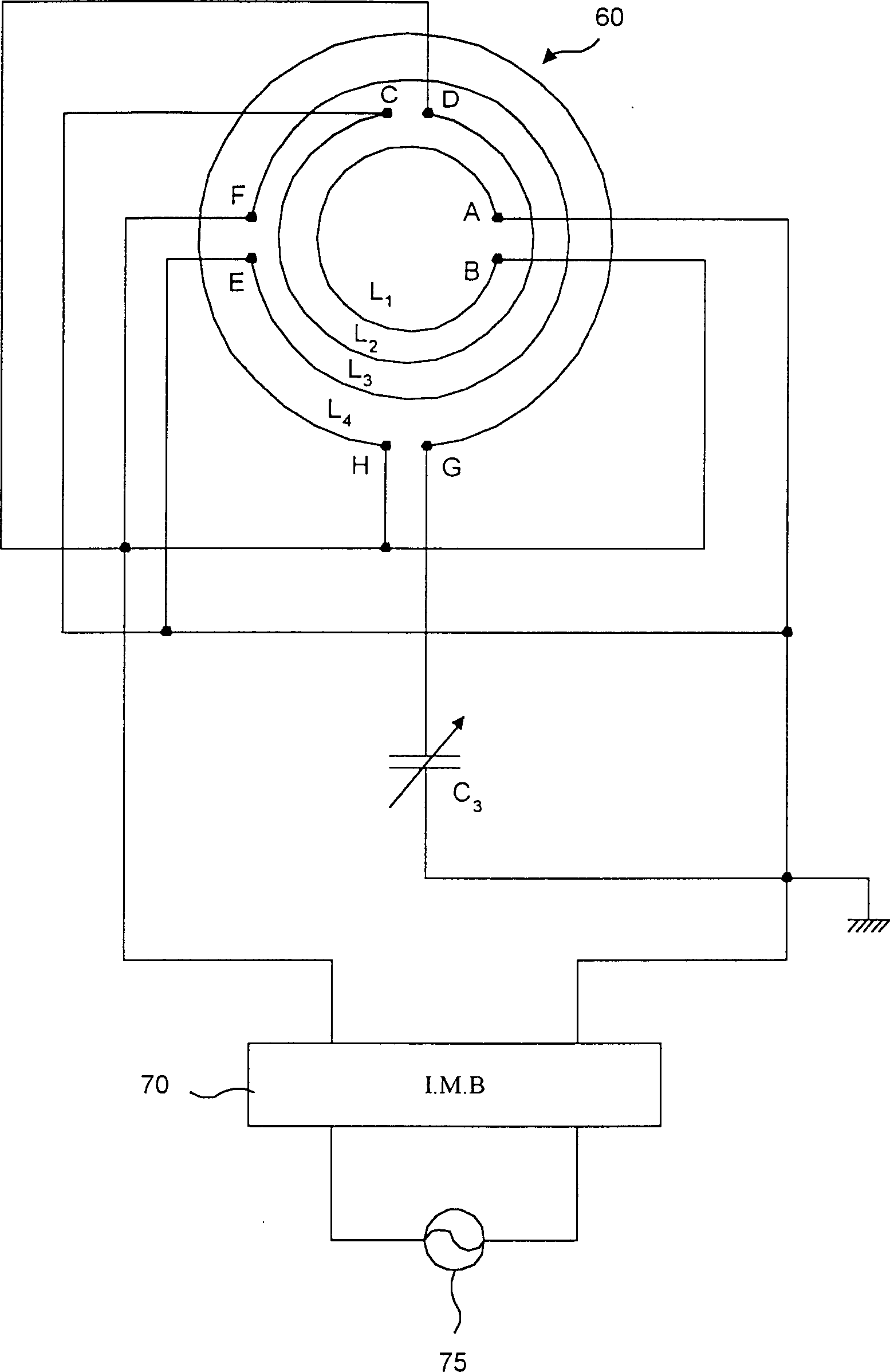
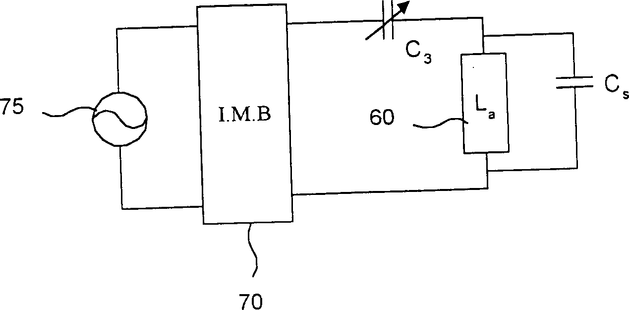
[0026] Figures 2a to 2c is a schematic diagram showing a VHF parallel resonant antenna according to the present invention. Specifically, Figure 2a with 2b is a schematic diagram showing the positional relationship between the very high frequency (VHF) parallel resonant antenna 60' and the impedance matching box 70, Figure 2c represents the equivalent circuit diagram, which includes the Figure 2a with 2b in the parasitic capacitance.

[0027] see Figures 2a to 2c , VHF parallel resonant anten...


PUM


Abstract

Disclosed is a plasma process apparatus in which a semiconductor device manufacturing process using a plasma is performed. The apparatus includes: a vacuum chamber in which a semiconductor device manufacturing process is performed; a very high frequency (VHF) power source for generating a VHF power; a VHF parallel resonance antenna having a plurality of antenna coils connected in parallel to each other, and multiple variable capacitors insertion-installed in series in the antenna coils, the antenna being installed at an outer upper portion of the vacuum chamber, and supplied with the VHF power from the VHF power source; and an impedance matching box for impedance matching between the VHF power and the VHF parallel resonance antenna. Preferably, the variable capacitor is a coaxial capacitor including: a first insulator tube; first two metal tubes respectively extending from both ends of the first insulator tube; a second insulator tube surrounding the first insulator tube, and partially surrounding the first two metal tubes placed adjacent to both sides thereof; and a second metal tube surrounding the second insulator tube, and installed so as to glide along an outer side surface of the second insulator tube.

Description

field of invention [0001] The present invention relates to plasma processing equipment, and more particularly, to inductively coupled plasma processing equipment with very high frequency parallel resonant antennas. Background technique [0002] In the manufacturing process of a semiconductor device, a process using plasma is often performed. Dry etching, chemical vapor deposition (CVD) and sputtering are examples of these processes. To reconsider the efficiency of these processes, ion concentrations of 1 × 10 11 ~2×10 11 ion / cm 3 high density plasma (HDP). It is known that such high density plasmas can be obtained by inductively coupled plasma (ICP). [0003] Figure 1a is a schematic diagram showing a conventional inductively coupled plasma processing apparatus. [0004] Referring to FIG. 1 a , a wafer chuck 20 is placed in the vacuum chamber 10 . Wafer 30 is loaded on wafer chuck 20 . The vacuum chamber 10 has a gas injection hole 12 and a gas discharge hole 14 . T...

Claims


Application Information

Patent Timeline
Patent Type & Authority Applications(China)
IPC IPC(8): H01L21/3065H01J37/32
CPCH01J37/32174H01J37/321H01L21/3065
Inventor 权奇清边洪植李承原金洪习韩淳锡高富珍金祯植
Owner JUSUNG ENG
Why Eureka
Try Eureka