Display assembly and assembling method thereof

An assembly method and display technology, applied to static indicators, parts of electrical measuring instruments, instruments, etc., can solve problems such as damage to the quality of display components

Inactive Publication Date: 2004-11-03
AU OPTRONICS CORP
View PDF0 Cites 18 Cited by
  • Summary
  • Abstract
  • Description
  • Claims
  • Application Information

AI Technical Summary

Problems solved by technology

Therefore, when the TCP pin 140 is bonded to the ITO pin 111 of the glass substrate 110, at the blocking area 139, the copper wire pattern layer 122 of the TCP tape and reel carrier package pin 140 will be separated from ...

Method used


Image

  • Display assembly and assembling method thereof
  • Display assembly and assembling method thereof
  • Display assembly and assembling method thereof

Examples


Embodiment Construction

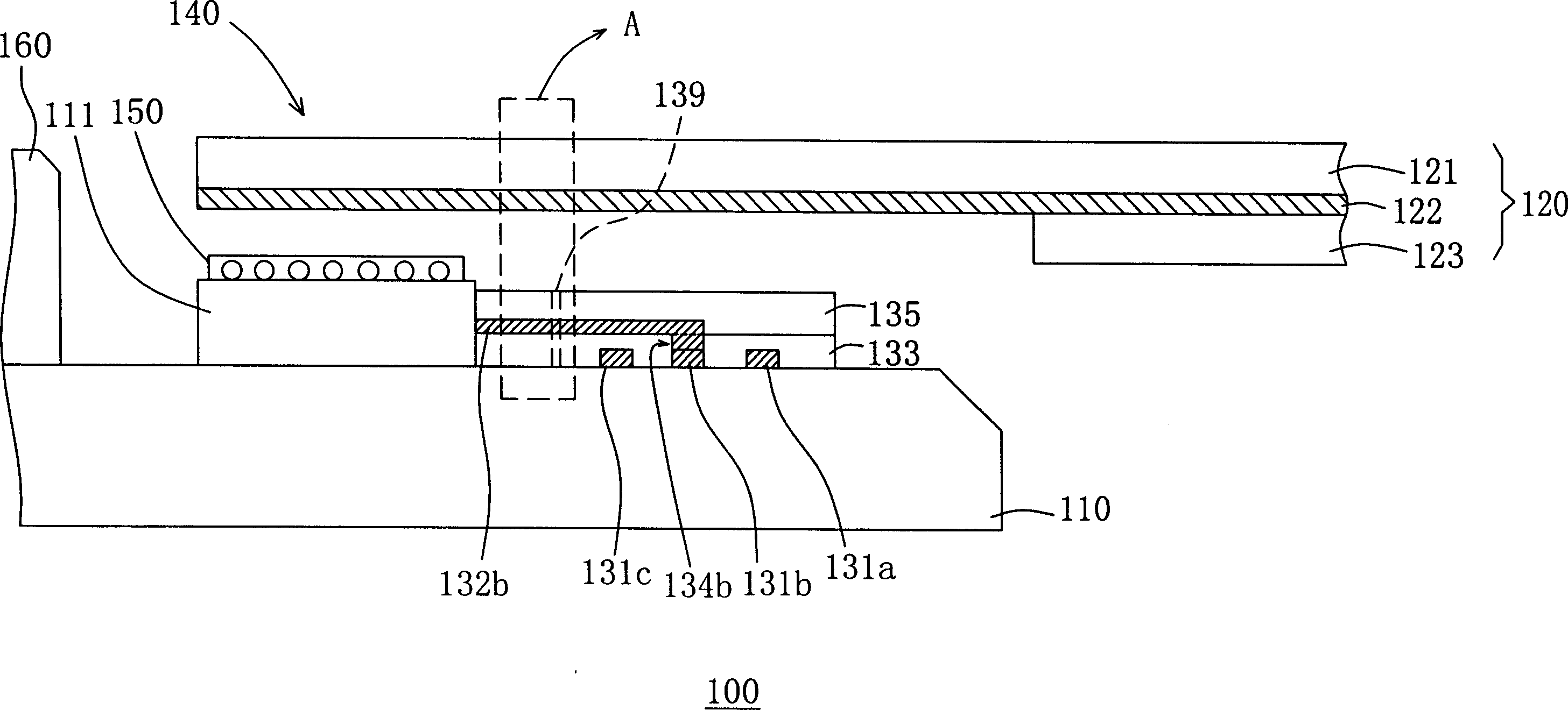
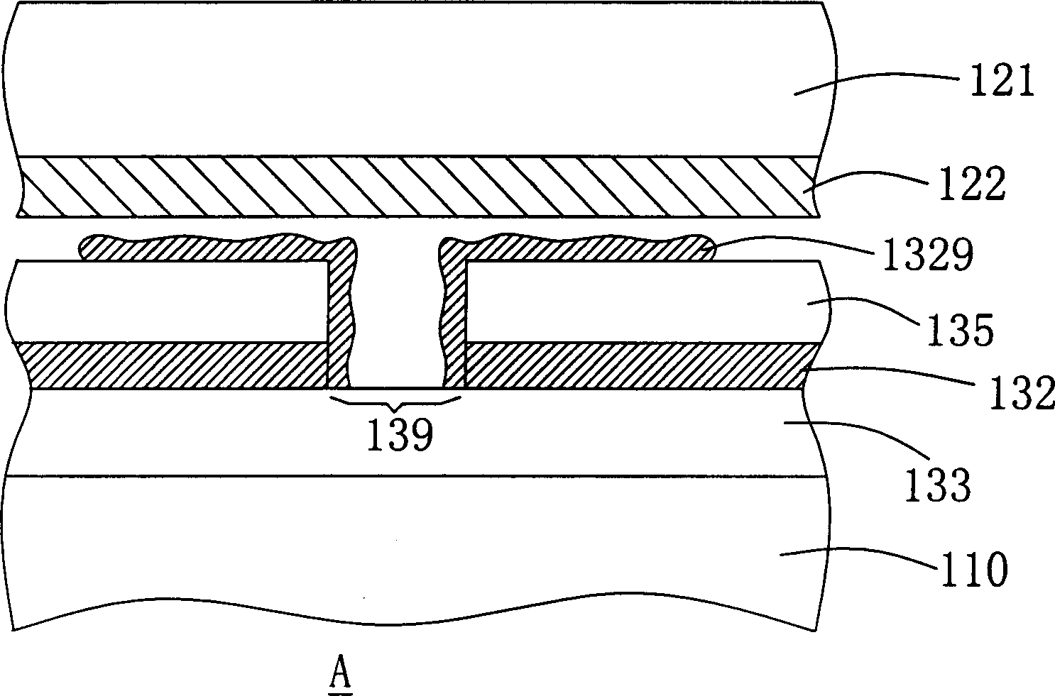
[0018] Please refer to figure 2 , which is a cross-sectional view of a display component according to a preferred embodiment of the present invention. exist figure 2 Among them, the display assembly 200 includes a glass substrate 210 , a tape carrier package (TCP) 220 and a protective insulating layer 290 . The display component 200 is, for example, a liquid crystal display component, and the glass substrate 210 is, for example, a glass substrate of a TFT substrate.

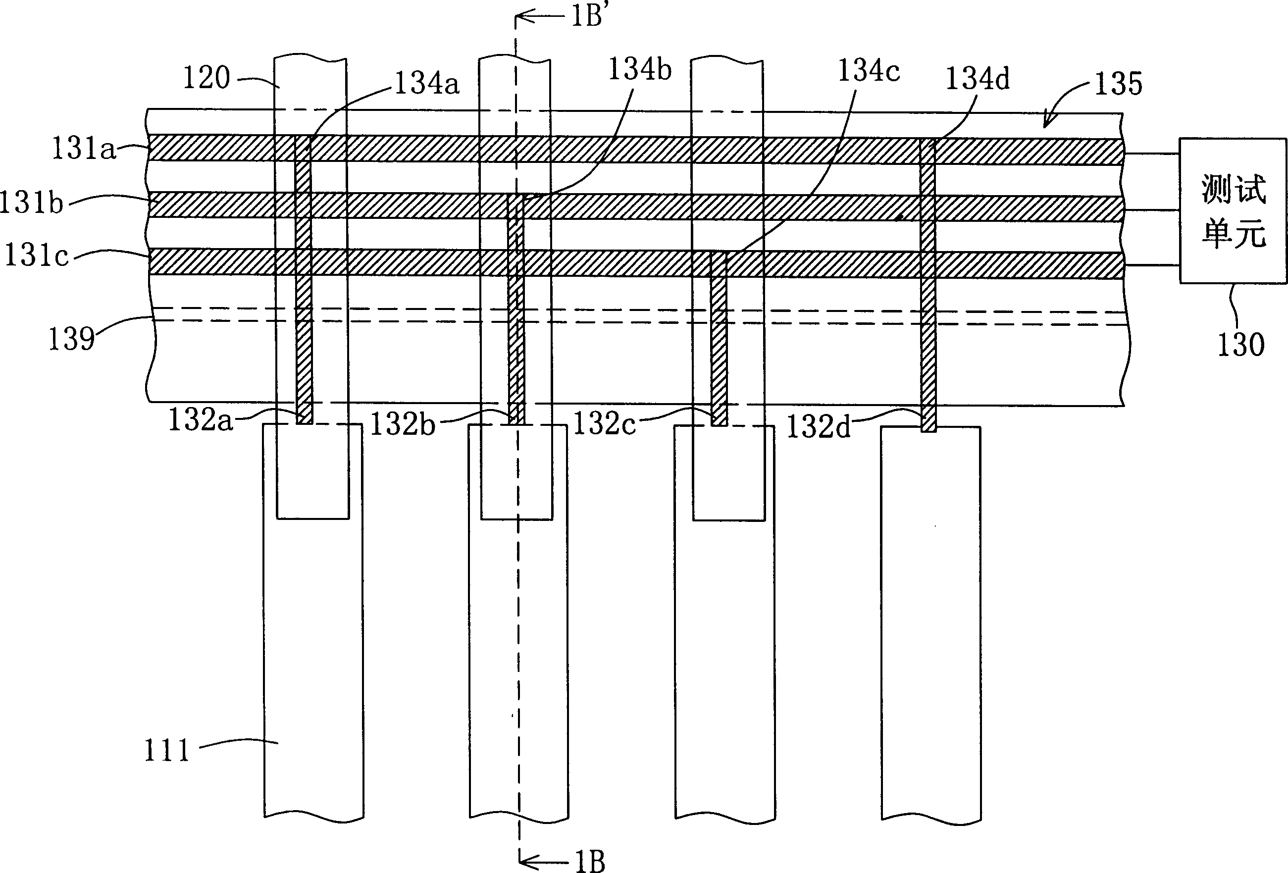
[0019] The glass substrate 210 has a display area 260, a plurality of indium tin oxide (Indium Tin Oxide, ITO) pins 211, and is equipped with a plurality of shorting bars, such as wires 231a, 231b, and 231c, and a plurality of wires. ,At figure 2 Only the wire 232b is used for illustration.

[0020] An insulating layer (Passivation Layer, PL) 233 is covered on the wires 231a, 231b and 231c. The wiring 232 b is located on the insulating layer 233 , and the wiring 232 b is covered with an insulating layer 2...


PUM


Abstract

The display assembly includes one glass substrate, one tape carrier package (TCP) and one protective insulating layer. The glass substrate is provided with a display area, lines and wires connected to one test unit. During test, the display area is connected via lines and wires for the test unit to test on the display area. After test, the wires are blocked and the glass substrate is not connected to the test unit. Only after the blocking area is formed, the protective insulating layer is formed on the glass substrate to cover the blocking area, and TCP is connected electrically with the glass substrate. The present invention can prevent TCP from contacting residual metal in the blocking area and prevent short circuit, and this raises the quality of the display.

Description

(1) Technical field [0001] The invention relates to a display unit, and more particularly to a display unit having a protective insulating layer to avoid short circuits. (2) Background technology [0002] For the general liquid crystal display (liquid crystal display, LCD) process, the general pre-process method is to perform a function test on the TFT substrate after the polarizer is attached to the thin film transistor (Thin Film Transistor, TFT) substrate. When the tested TFT substrate is defective, it must be discarded, which often causes the attached polarizer to be discarded, resulting in waste of the polarizer. In order to avoid waste of raw materials and save manufacturing costs, after the first cutting of the TFT substrate and before attaching the polarizer, a 2G3D or 2G2D pre-test (pre-test) is performed on the TFT substrate to screen out defective products first. TFT substrate. [0003] Please also refer to Figure 1A and Figure 1B . Figure 1A is a partial sc...

Claims


Application Information

Patent Timeline
IPC IPC(8): G01R1/02G01R3/00G02F1/133
Inventor 陈慧昌杨金城
Owner AU OPTRONICS CORP
Why Eureka
Try Eureka