Device test apparatus and test method

A test equipment and test unit technology, applied in semiconductor/solid-state device testing/measurement, single semiconductor device testing, electrical solid-state devices, etc. The effect of improving efficiency and high test efficiency

Inactive Publication Date: 2005-02-02
SHARP KK
View PDF1 Cites 22 Cited by
  • Summary
  • Abstract
  • Description
  • Claims
  • Application Information

AI Technical Summary

Problems solved by technology

Also, the transmission time of the test results obtained in each test unit and the waiting time until the test results are transmitted increase due to the influence of the communication time and the increase of the processing time.
As a result, there is a problem of reduced test efficiency, which affects mass production

Method used


Image

  • Device test apparatus and test method
  • Device test apparatus and test method
  • Device test apparatus and test method

Examples


Embodiment Construction

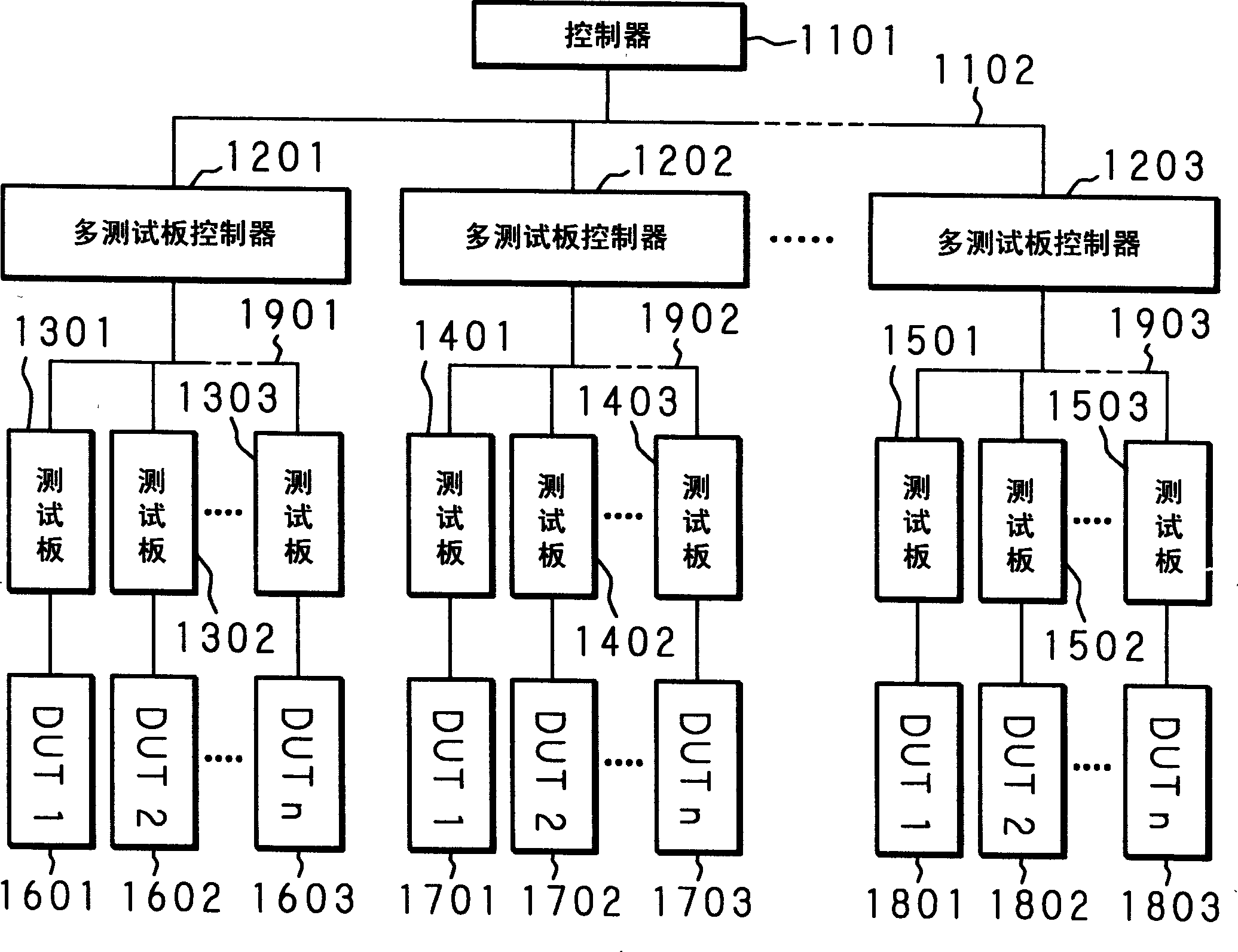
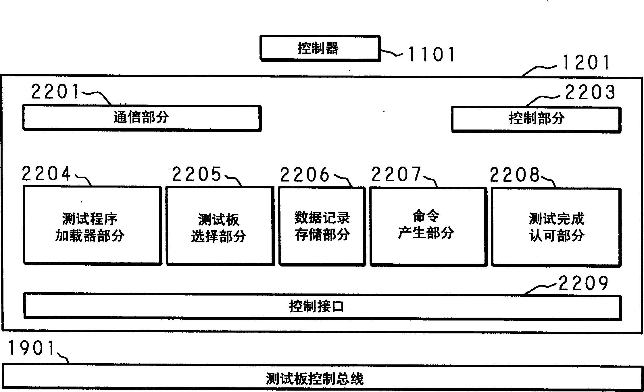
[0024] Hereinafter, the present invention will be described in detail with reference to the accompanying drawings that illustrate embodiments of the invention. Figure 2 to Figure 5B A testing device according to the invention is described, inter alia, figure 2 shows the overall structure of the present invention, image 3 shown figure 2 shows the internal structure of the multi-test board controller, Figure 4 shown figure 2 shows the internal structure of the test board, and Figure 5A and Figure 5B Shows the connection status of the multi-board controller to the test board.

[0025] Such as figure 2 Shown, the test equipment for the device under test such as semiconductor integrated circuit of the present invention comprises: a controller 1101; As a plurality of multi-test board controllers 1201-1203 of control unit; And be connected to respective multi-test board as test unit Multiple test boards 1301-1303, 1401-1403, 1501-1503 of controllers 1201-1203. The co...


PUM


Abstract

One test board for executing a test is provided for each of a plurality of DUTs (Devices-Under-Test) such as semiconductor integrated circuits, a multi test board controller for managing these test boards is provided, and a plurality of test boards managed by each multi test board controller are operated in parallel to simultaneously perform independent tests on the respective DUTs.

Description

technical field [0001] The present invention relates to a kind of equipment and method for testing devices under test, such as semiconductor integrated circuits such as large scale integration (LSI) wafers, and more particularly to a testing device and a testing method capable of performing independent tests on many devices under test at the same time . Background technique [0002] Conventionally, multiple devices under test are independently tested simultaneously (for example, Japanese Utility Model Application Laid-Open No. 64-47148 / 1989). figure 1 is a block diagram of a conventional test device disclosed in Japanese Utility Model Application Laid-Open No. 64-47148 / 1989. The test equipment includes: a plurality of test units 31-33 controlled by a microprocessor that has stored a test program that operates independently; processing with a monitoring function and a human-machine interface function for monitoring the operating conditions of each test unit 31-33 processor ...

Claims


Application Information

Patent Timeline
Patent Type & Authority Applications(China)
IPC IPC(8): G01R31/26G01R31/28G01R31/319H01L21/66
CPCG01R31/2851G01R31/31926G01R31/2834G07F19/201G07D2211/00
Inventor 松本享三
Owner SHARP KK
Why Eureka
Try Eureka