Solid-state image pickup device

An imaging device and solid-state technology, applied in the field of solid-state imaging devices, can solve the problems of performance degradation of solid-state imaging devices, inability to improve interface states and lattice disorder, etc.

Inactive Publication Date: 2005-02-02
SONY CORP
View PDF3 Cites 12 Cited by
  • Summary
  • Abstract
  • Description
  • Claims
  • Application Information

AI Technical Summary

Problems solved by technology

As a result, the above-mentioned interface state and disorder of the crystal lattice cannot be improved, and therefore, the performance of the solid-state imaging device 30 is lowered.

Method used


Image

  • Solid-state image pickup device
  • Solid-state image pickup device
  • Solid-state image pickup device

Examples


Embodiment Construction

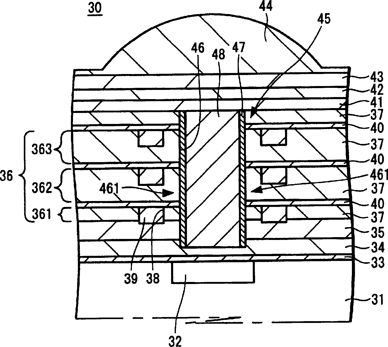
[0064] Referring to the drawings, a solid-state imaging device according to an embodiment of the present invention will now be described. image 3 A schematic configuration of a solid-state imaging device in which the present invention is applied to a CMOS type solid-state imaging device (CMOS sensor) is shown.

[0065] More specifically, image 3 is a cross-sectional view showing one pixel portion of a CMOS type solid-state imaging device according to an embodiment of the present invention.

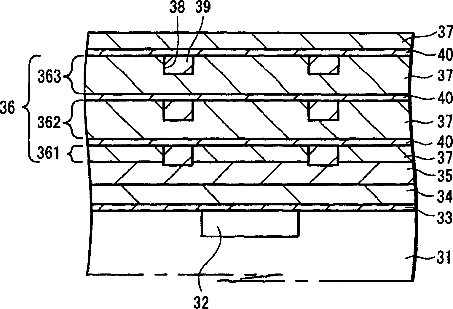
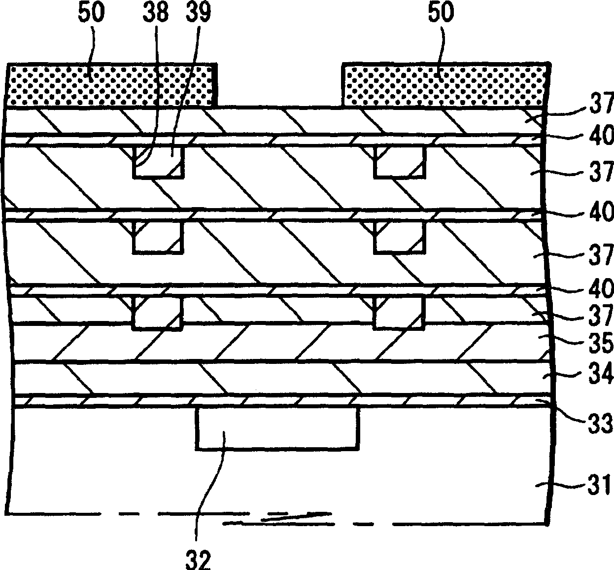
[0066] usually as image 3 A CMOS type solid-state imaging device denoted by reference numeral 100 in includes a semiconductor substrate 1 . A light-receiving sensor portion 2 is formed at a predetermined position in a semiconductor substrate 1, and a silicon oxide film (SiO film) 3, for example, having an insulating function, a surface protecting function, or a surface planarizing function is formed on the semiconductor substrate 1. A silicon nitride film (SiN film) 4 having a surfac...


PUM


Abstract

A solid-state image pickup device (100) is constructed in which a waveguide (15) is formed in an insulating layer on a light-receiving sensor portion (2), a side wall (161) of the waveguide (15) is covered with a reflective film (17) made of an Al film deposited by a CVD method, an underlayer film (19) is formed between the reflective film (17) and the side wall (161) of the waveguide (15) and the underlayer film (19) is made of a VIa-group element. It is possible to obtain a solid-state image pickup device including a waveguide in which hydrogen supplied to the light-receiving sensor portion (2) can be restrained from being absorbed by the underlayer film (19) and which has the reflective film (17) of high reflectivity with satisfactory surface condition, satisfactory coverage and excellent adhesion.

Description

technical field [0001] The present invention relates to a solid-state imaging device, and more particularly to a solid-state imaging device in which a light-receiving sensor portion has a waveguide provided thereon to increase the focusing efficiency of incident light on the light-receiving sensor portion. Background technique [0002] A CCD (charge-coupled device, charge-coupled device) or CMOS (complementary metal-oxide-semiconductor, complementary metal oxide semiconductor) type solid-state imaging device in most cases has a configuration in which an on-chip microlens ( on-chip microlens) is provided via an insulating layer on a plurality of light-receiving sensor parts composed of photodiodes, such as pixels, so that the focus of incident light passing through the on-chip microlens is close to the light-receiving sensor part, thereby guiding Light enters the light receiving sensor section. [0003] However, as the pixel size decreases and the multilayer wiring layer inc...

Claims


Application Information

Patent Timeline
Patent Type & Authority Applications(China)
IPC IPC(8): H01L27/14H01L27/00H01L27/146H01L31/00H01L31/0232H04N5/225
CPCH01L27/14636H01L27/14625H01L27/14629H01L27/14656H01L27/14623H01L27/146H01L27/14
Inventor 高桥新吾榎本容幸阿部秀司
Owner SONY CORP
Why Eureka
Try Eureka