Cascaded organic electroluminescent device having connecting units with n-type and p-type organic layers

A technology of electroluminescent devices and connection units, which is applied in the field of cascaded organic electroluminescent devices, can solve problems such as low output and complexity, and achieve the effects of simplifying production steps, improving light extraction, and high brightness

Active Publication Date: 2005-04-27
GLOBAL OLED TECH
View PDF69 Cites 23 Cited by
  • Summary
  • Abstract
  • Description
  • Claims
  • Application Information

AI Technical Summary

Problems solved by technology

Both methods are complex and result in low yield

Method used


Image

  • Cascaded organic electroluminescent device having connecting units with n-type and p-type organic layers
  • Cascaded organic electroluminescent device having connecting units with n-type and p-type organic layers
  • Cascaded organic electroluminescent device having connecting units with n-type and p-type organic layers

Examples


Embodiment 1

[0175] Embodiment 1 (traditional OLED-comparison)

[0176] A conventional non-cascaded OLED was prepared as follows: an approximately 1.1 mm thick glass substrate coated with a transparent ITO conductive layer was cleaned and dried with an industrial glass washer. The thickness of ITO was about 42 nm and the sheet resistance of ITO was about 68 Ω / square. The ITO surface is then treated with an oxidizing plasma to make its surface available as an anode. By decomposing CHF in an RF plasma processing chamber 3 gas, a 1 nm thick layer of CFx was deposited on a clean ITO surface as a HIL. The substrate was then transferred to a vacuum deposition chamber to deposit all other layers on top of the substrate. at about 10 -6 Under the torg vacuum degree, the following layers are sequentially deposited in the following order through the sublimation of the heated dish:

[0177] (1) HTL, 90nm thick, made of NPB;

[0178] (2) LEL, 20 nm thick, composed of Alq host doped with 1.0 vol% ...

Embodiment 2

[0187] Embodiment 2 (the present invention)

[0188] A cascaded OLED with two EL units was fabricated as follows: an approximately 1.1 mm thick glass substrate coated with a transparent ITO conductive layer was cleaned and dried with an industrial glass washer. The thickness of ITO was about 42 nm and the sheet resistance of ITO was about 68 Ω / square. The ITO surface is then treated with an oxidizing plasma to make its surface available as an anode. By decomposing CHF in an RF plasma processing chamber 3 gas, a 1 nm thick layer of CFx was deposited on a clean ITO surface as a HIL. The substrate was then transferred to a vacuum deposition chamber to deposit all other layers on top of the substrate. at about 10 -6 Under the torg vacuum degree, the following layers are sequentially deposited in the following order through the sublimation of the heated dish:

[0189] (1) The first HTL, 60nm thick, made of NPB, acts as a spacer between the transparent anode and the first EL ...

Embodiment 3

[0206] Embodiment 3 (the present invention)

[0207] Except that step (5)-step (9) is repeated once after embodiment 2 step (9) to increase a connection unit and an EL unit, then carry out steps (10) and (11), according to the same method as embodiment 2 A cascaded OLED with three EL units was fabricated.

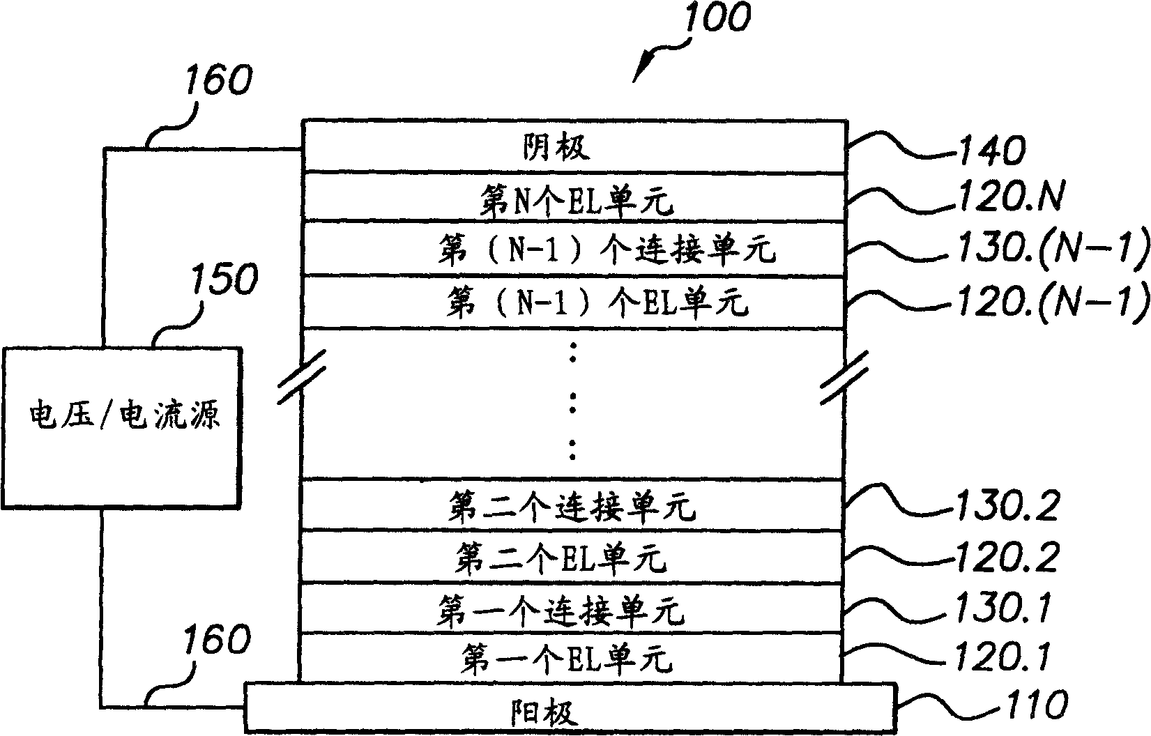
[0208] After the layers were deposited, the device was transferred from the deposition chamber to a dry box for sealing. The complete device structure is defined as ITO / CFx / NPB(60) / EL / CU / EL / CU / EL / Alq(30) / Mg:Ag.

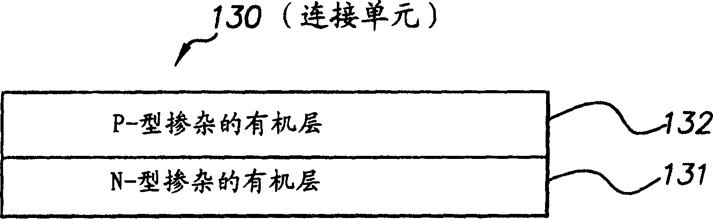
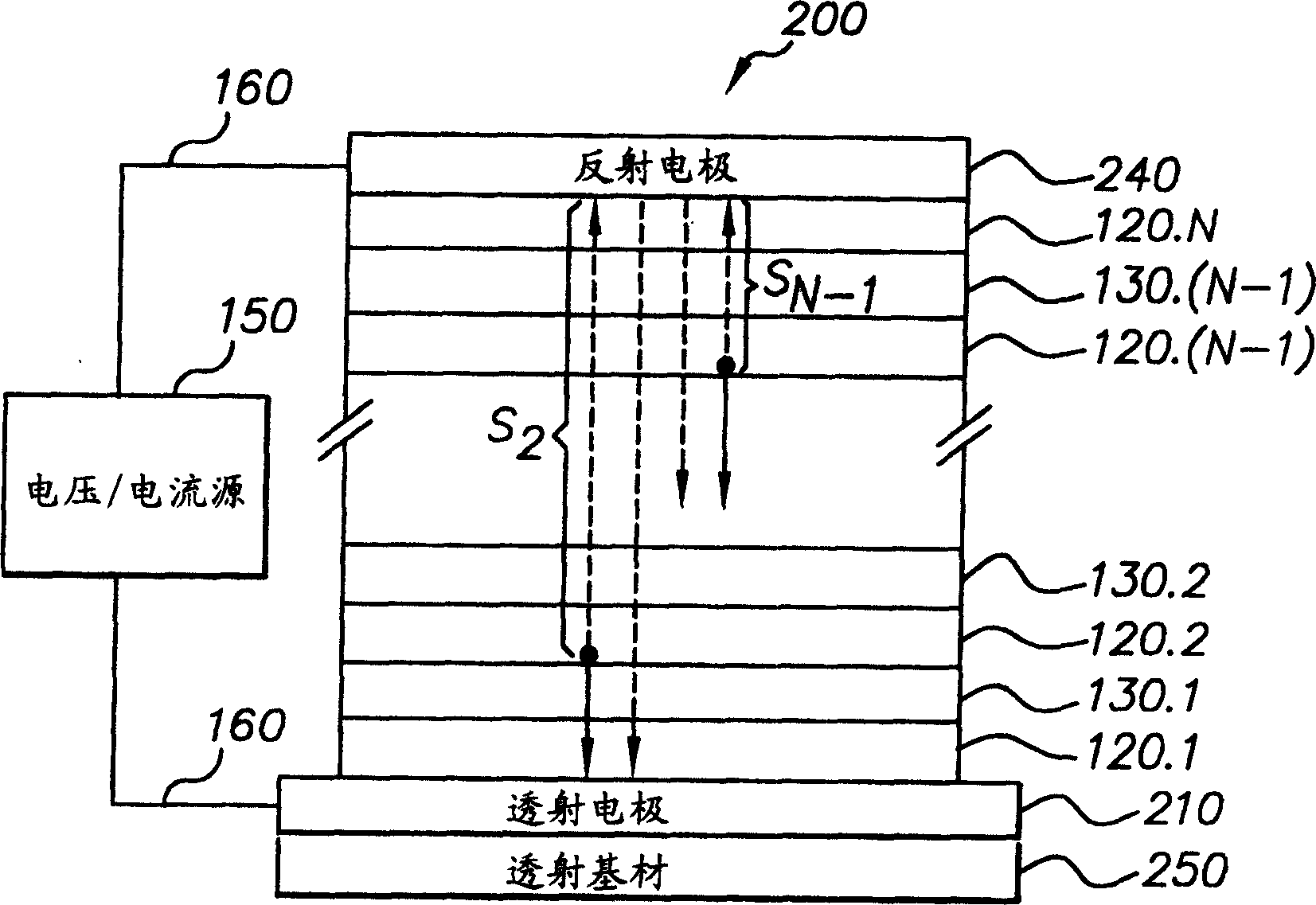
[0209] Same as Example 2, in this cascaded OLED, the resistivity of the connection unit is higher than 10Ω-cm and the light transmittance is higher than 90%. The emission peak wavelength λ of each LEL is 524 nm. S 3 = S 3,O =95nm, S 2 =1.01×S 2,O = 362nm, and S 1 =1.02×S 1,O = 1.02 x 619 = 629 nm. The optical distance between each emission center plane and the Mg:Ag reflective cathode was optimized. Furthermore, the physical separation between each emiss...


PUM


Abstract

A cascaded organic electroluminescent device includes an anode and a cathode. The device also includes a plurality of organic electroluminescent units disposed between the anode and the cathode, wherein the organic electroluminescent units comprise at least a hole-transporting layer, an electron-transporting layer, and an electroluminescent zone formed between the hole-transporting layer and the electron-transporting layer wherein the physical spacing between adjacent electroluminescent zones is more than 90 nm; and a connecting unit disposed between each adjacent organic electroluminescent unit, wherein the connecting unit comprises, in sequence, an n-type doped organic layer and a p-type doped organic layer forming a transparent p-n junction structure wherein the resistivity of each of the doped layers is higher than 10 OMEGA -cm.

Description

technical field [0001] The present invention relates to providing a plurality of organic electroluminescent units to form a cascaded organic electroluminescent device. Background technique [0002] Organic electroluminescent (EL) devices or organic light emitting (OLED) devices are electronic devices that emit light in response to an applied electrical potential. The structure of an OLED includes an anode, an organic EL medium, and a cathode in sequence. An organic EL medium located between an anode and a cathode usually consists of an organic hole transport layer (HTL) and an organic electron transport layer (ETL). The holes and electrons recombine in the ETL near the HTL / ETL interface and emit light. Tang et al. ["Organic Electroluminescent Diodes", Applied Physics Letters, 51, 913 (1987), and co-cited US-A-4,769,292] demonstrated very high efficiencies in OLEDs employing the layer structure described above. Various OLEDs with alternating layer structures have subsequen...

Claims


Application Information

Patent Timeline
Patent Type & Authority Applications(China)
IPC IPC(8): H05B33/12H01L27/32H01L51/50H01L51/52H05B33/18
CPCH01L51/5278H10K50/19A44C5/2076A44C15/005
Inventor 廖良生K·P·克卢贝克D·L·康福特邓青云
Owner GLOBAL OLED TECH
Why Eureka
Try Eureka