Lithographic apparatus and device manufacturing method

A lithographic projection and beam technology, applied in the field of device manufacturing, can solve problems such as reducing image quality

Active Publication Date: 2005-07-13
ASML NETHERLANDS BV
View PDF4 Cites 46 Cited by
  • Summary
  • Abstract
  • Description
  • Claims
  • Application Information

AI Technical Summary

Problems solved by technology

[0009] This new technique has undesired disadvantages when compared to systems without liquid in the exposure radiation path
In particular, while improving imaging resolution, liquids otherwise tend to degrade image quality

Method used


Image

  • Lithographic apparatus and device manufacturing method
  • Lithographic apparatus and device manufacturing method
  • Lithographic apparatus and device manufacturing method

Examples


Embodiment 1

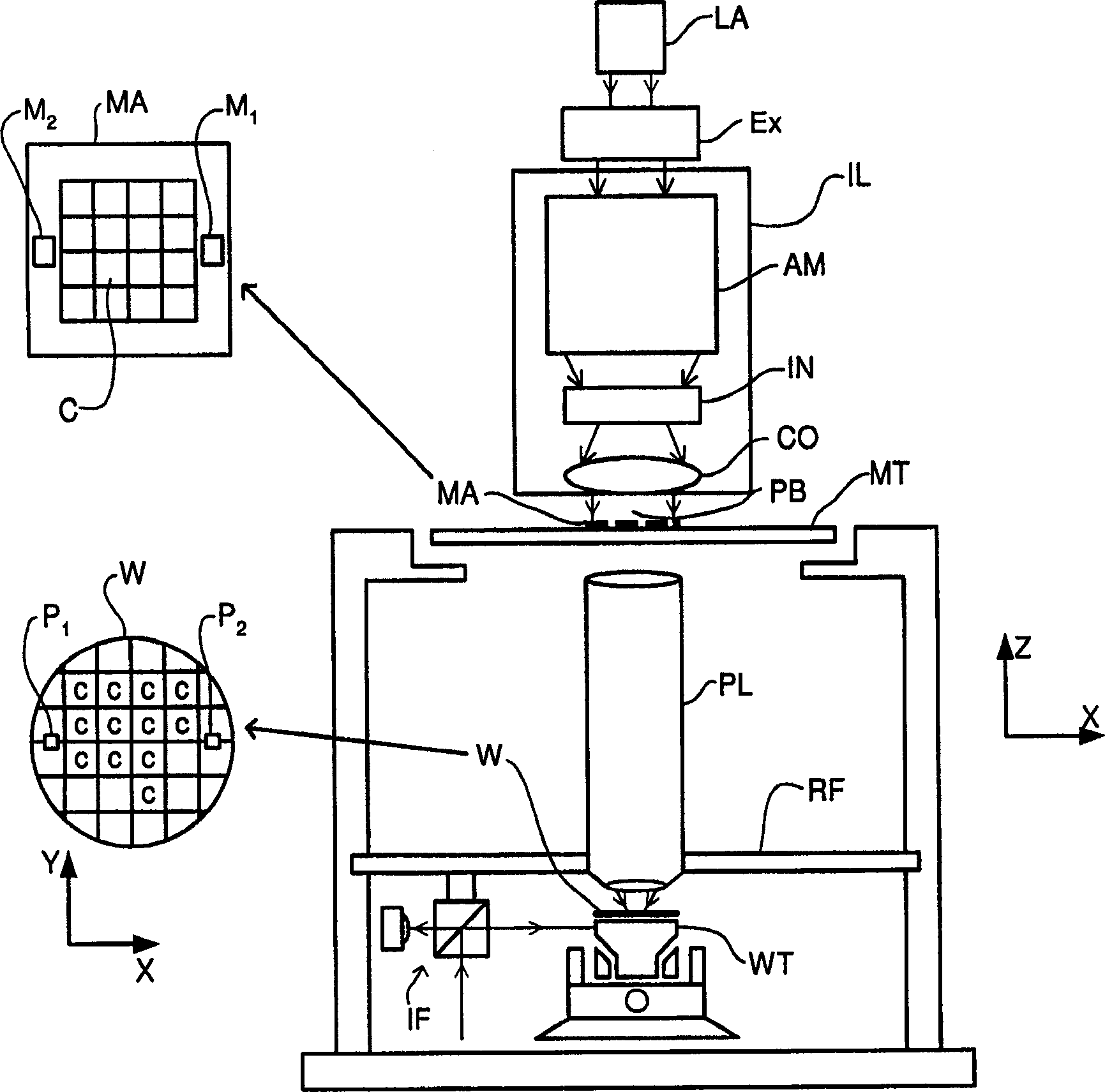
[0088] figure 1 A photolithographic apparatus according to a specific embodiment of the present invention is schematically shown. The unit includes:

[0089] - An illumination system (illuminator) IL for providing a radiation projection beam PB (eg UV radiation or DUV radiation).

[0090] - a first support structure (eg mask table) MT for supporting the patterning device (eg mask) MA and connected to first positioning means PM for precise positioning of the patterning device relative to the object PL;

[0091] - a substrate table (e.g. a wafer table) WT for holding a substrate (e.g. a resist-coated wafer) W and connected to a second positioning device PW for precise positioning of the substrate relative to the object PL;

[0092] - A projection system (eg a refractive projection lens) PL for imaging the pattern imparted to the projection beam PB onto a target portion C (eg comprising one or more dies) of the substrate W by means of the patterning device MA.
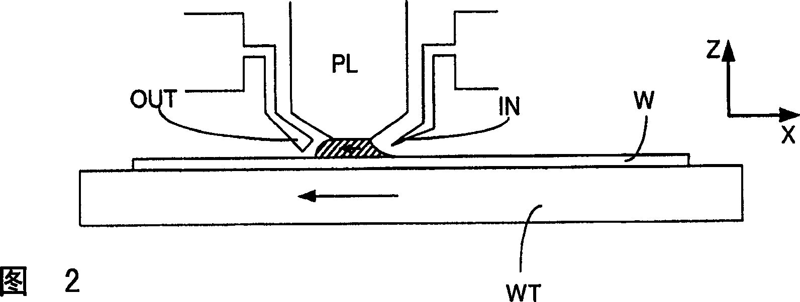
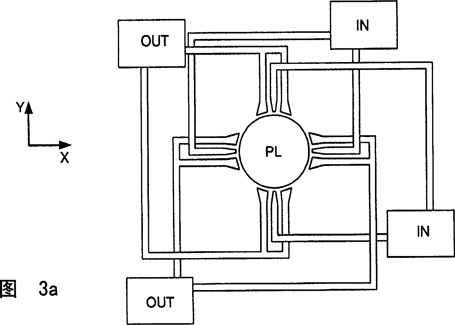
[0093] As ind...


PUM

PropertyMeasurementUnit
diameteraaaaaaaaaa

Abstract

A lithographic apparatus and device manufacturing method using a high refractive index liquid confined in a container (13) which at least partially fills the imaging region between the final element of the projection lens and the substrate. Bubbles formed in a liquid in which atmospheric gases are dissolved or outgassed from a device element exposed to the liquid are detected and removed so that the bubbles do not interfere with exposure to cause print defects on the substrate. Detection is performed by measuring frequencies related to ultrasonic attenuation in liquids, by degassing and pressurizing liquids, isolating liquids from the atmosphere, using liquids with low surface tension, providing continuous flow of liquid through the imaging area, and phase shifting Ultrasonic standing wave nodal pattern for air bubble removal.

Description

technical field [0001] The invention relates to a photolithography device and a device manufacturing method. Background technique [0002] A lithographic projection device is a device that projects a desired pattern onto a target portion of a substrate. The lithographic apparatus can be used, for example, in the manufacture of integrated circuits (ICs). In this case, a patterning device such as a mask can be used to create a circuit pattern corresponding to an individual layer of the IC that can be imaged on a target portion of the substrate (silicon wafer) that has been coated with a layer of radiation-sensitive material (resist) on (eg, including one or more dies). In general, a single substrate will contain the entire grid of adjacent target portions which are successively irradiated one by one by the projection system. Known lithographic apparatuses include so-called steppers, in which each target portion is irradiated by exposing the entire pattern on the target port...

Claims


Application Information

Patent Timeline
Patent Type & Authority Applications(China)
IPC IPC(8): G03F7/20H01L21/027
CPCG03F7/70341G03F7/70858G03F7/20G03F7/708
Inventor J·T·德斯米特V·Y巴尼内T·H·J·比斯肖普斯T·M·莫德曼M·M·T·M·迪里奇斯
Owner ASML NETHERLANDS BV
Why Eureka
Try Eureka