Film formation method

A film-forming method and film-forming technology, which are applied in the fields of electrical components, semiconductor/solid-state device manufacturing, circuits, etc., and can solve problems such as the inability to confirm the change of gas pressure and the change of film thickness

Inactive Publication Date: 2005-07-20
TOKYO ELECTRON LTD
View PDF0 Cites 1 Cited by
  • Summary
  • Abstract
  • Description
  • Claims
  • Application Information

AI Technical Summary

Problems solved by technology

Therefore, when both the atmospheric pressure and the gas pressure (absolute pressure) in the heat treatment furnace change, the change in the gas pressure in the heat t

Method used


Image

  • Film formation method
  • Film formation method
  • Film formation method

Examples


Embodiment approach

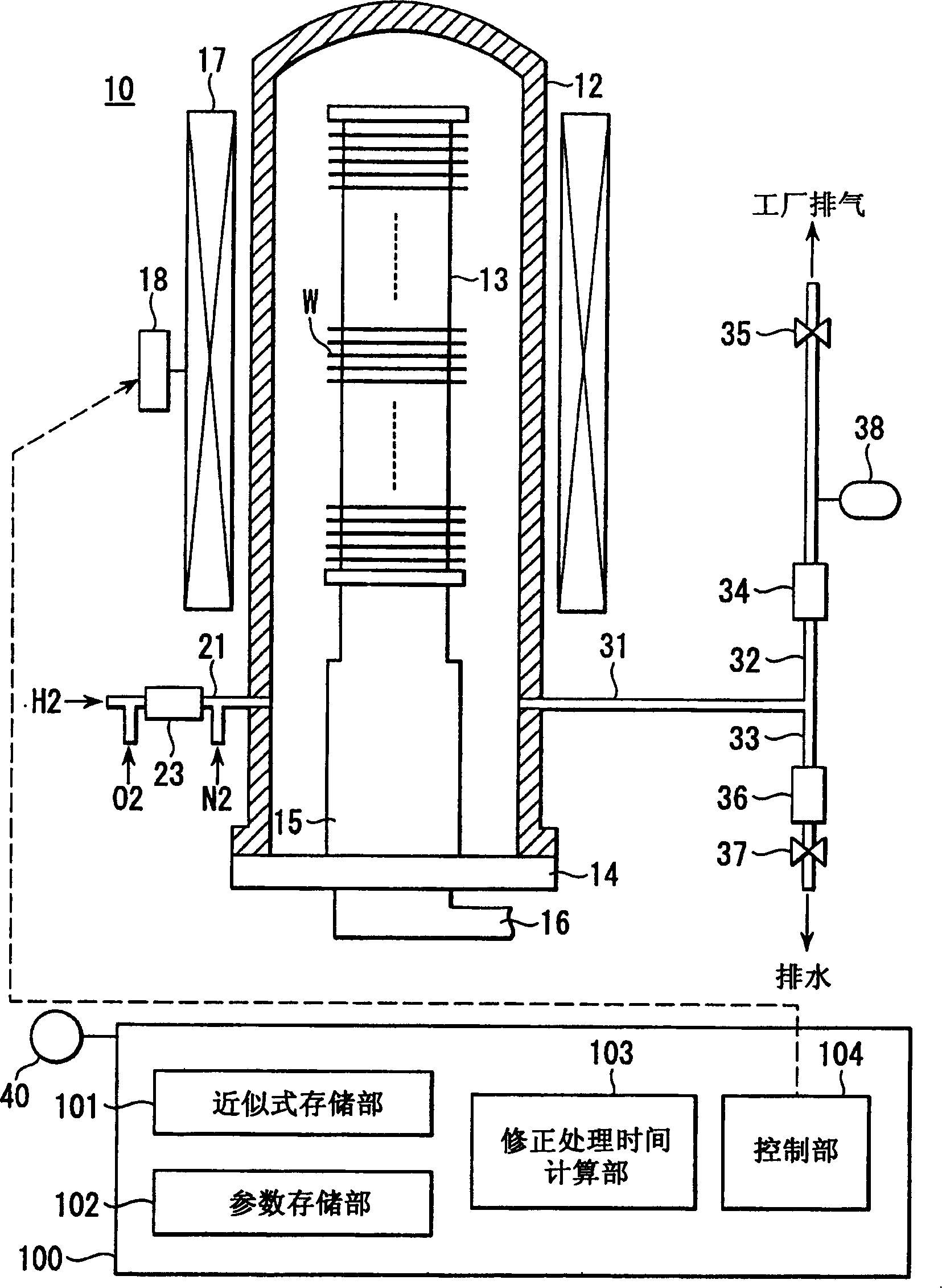
[0019] figure 1 It is a sectional view showing part of a vertical heat treatment apparatus as a film formation apparatus for semiconductor processing according to an embodiment of the present invention. Such as figure 1 As shown, a vertical heat treatment apparatus 10 has a reaction tube 12 made of, for example, quartz and plugged at the upper end. In the reaction tube 12, a plurality of, for example, 150 semiconductor wafers W (product wafers) serving as substrates are placed on the wafer carrier 13 as a holder in a shelf shape at regular intervals up and down in a horizontal state. The wafer carrier 13 is held by the lid body 14 via a thermal insulation cylinder (heat insulator) 15 .

[0020] The lid body 14 is placed on a carrier elevator 16 for carrying the wafer carrier 13 into or out of the reaction tube 12 . When at the upper limit position, the lid body 14 has the function of closing the lower end opening of the processing container constituted by the reaction tube ...


PUM


Abstract

A film formation method includes a preparation stage (S 10 ) and a process stage (S 20 ). In the preparation stage (S 10 ), a process time correction equation prepared to correct process time in accordance with atmospheric pressure is derived, based on a first relational equation that expresses a relationship between film thickness and process time, and a second relational equation that expresses a relationship between atmospheric pressure and film thickness (S 11 to S 14 ). In the process stage (S 20 ), process time is corrected, based on the process time correction equation thus derived and a measurement result of current atmospheric pressure, and then film formation is performed, based on process time thus corrected (S 21 to S 23 ).

Description

technical field [0001] The present invention relates to a film forming method, a method for deriving a correction formula for film forming processing time, a film forming apparatus, and a program for the deriving method. In particular, the present invention relates to improvement of a film-forming method for semiconductor processing. Here, "semiconductor processing" refers to the process of forming semiconductor layers, insulating layers, conductive layers, etc. Various processes performed on structures such as wiring and electrodes connected to semiconductor devices. Background technique [0002] In the semiconductor manufacturing process, one of the devices for forming films on semiconductor wafers is a vertical heat treatment device that performs batch processing. In such an apparatus, a plurality of wafers are held in a shelf shape in a holder such as a wafer carrier. Such a holder is carried into a vertical heat treatment furnace, and a reaction gas such as oxygen is...

Claims


Application Information

Patent Timeline
IPC IPC(8): H01L21/31H01L21/00
CPCH01L21/67253H01L21/31
Inventor 松浦广行高桥丰
Owner TOKYO ELECTRON LTD
Why Eureka
Try Eureka