
Liquid crystal display device built-in finger printing device and method of manufacturing the same

A liquid crystal display device and fingerprint technology, which is applied to static indicators, character and pattern recognition, and acquisition/organization of fingerprints/palmprints, etc., can solve problems such as difficulties in manufacturing process management, image quality degradation, and lower aperture ratio, and achieve improved Image display quality, ease of management, reduction in number of effects

Inactive Publication Date: 2005-10-26
SAMSUNG ELECTRONICS CO LTD
View PDF0 Cites 45 Cited by
  • Summary
  • Abstract
  • Description
  • Claims
  • Application Information

AI Technical Summary

Problems solved by technology

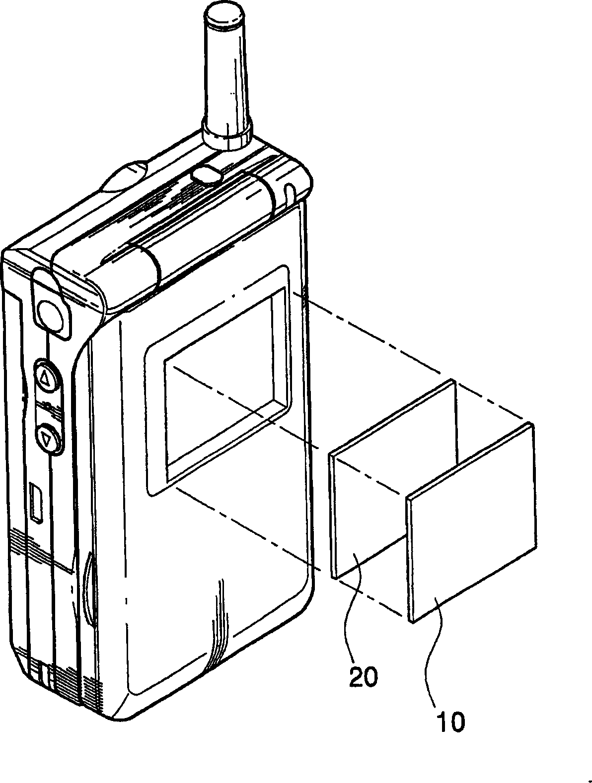
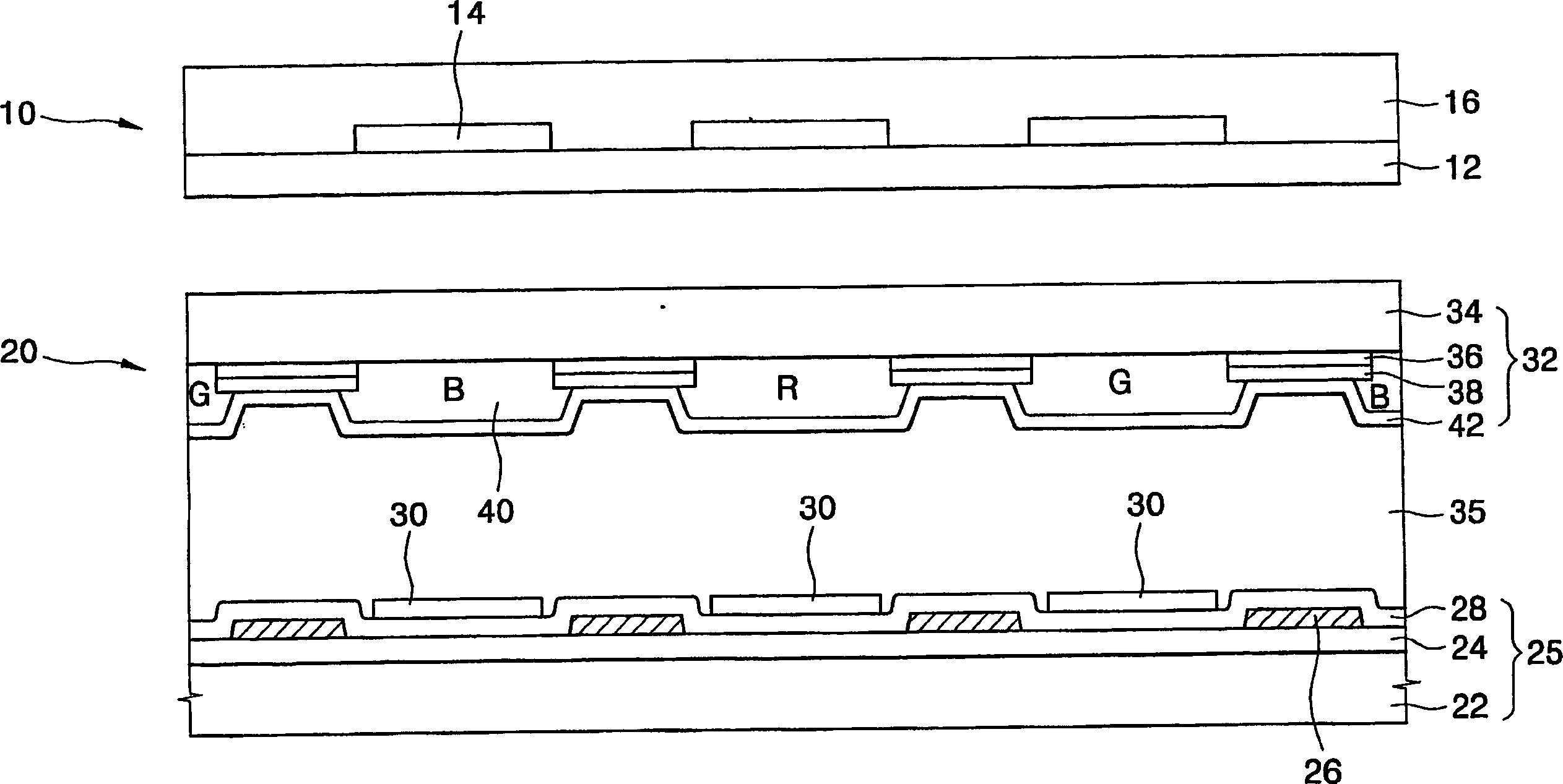
When the TFT fingerprint recognition substrate 10 is not precisely aligned with the TFT-LCD panel 20, the aperture ratio (aperture ratio) of the TFT fingerprint recognition substrate 10 may be reduced by n times compared with the aperture ratio of the TFT-LCD panel 20
[0016] In particular, when the TFT substrate 25 of the TFT-LCD panel 20 is not precisely aligned with the color filter substrate 32 of the TFT-LCD panel 20, the aperture ratio is greatly reduced.
Therefore, little design margin may be left and management of the manufacturing process may be difficult
[0017] In addition, the precise alignment process may not be easy to complete, and when designing the TFT-LCD panel 20 mounted with the TFT fingerprint identification substrate 10 considering the misalignment between the substrates, the image quality may be degraded due to the reduced aperture ratio

Method used


Image

  • Liquid crystal display device built-in finger printing device and method of manufacturing the same
  • Liquid crystal display device built-in finger printing device and method of manufacturing the same
  • Liquid crystal display device built-in finger printing device and method of manufacturing the same

Examples


Embodiment Construction

[0044] Hereinafter, preferred embodiments of the present invention will be described in detail with reference to the accompanying drawings.

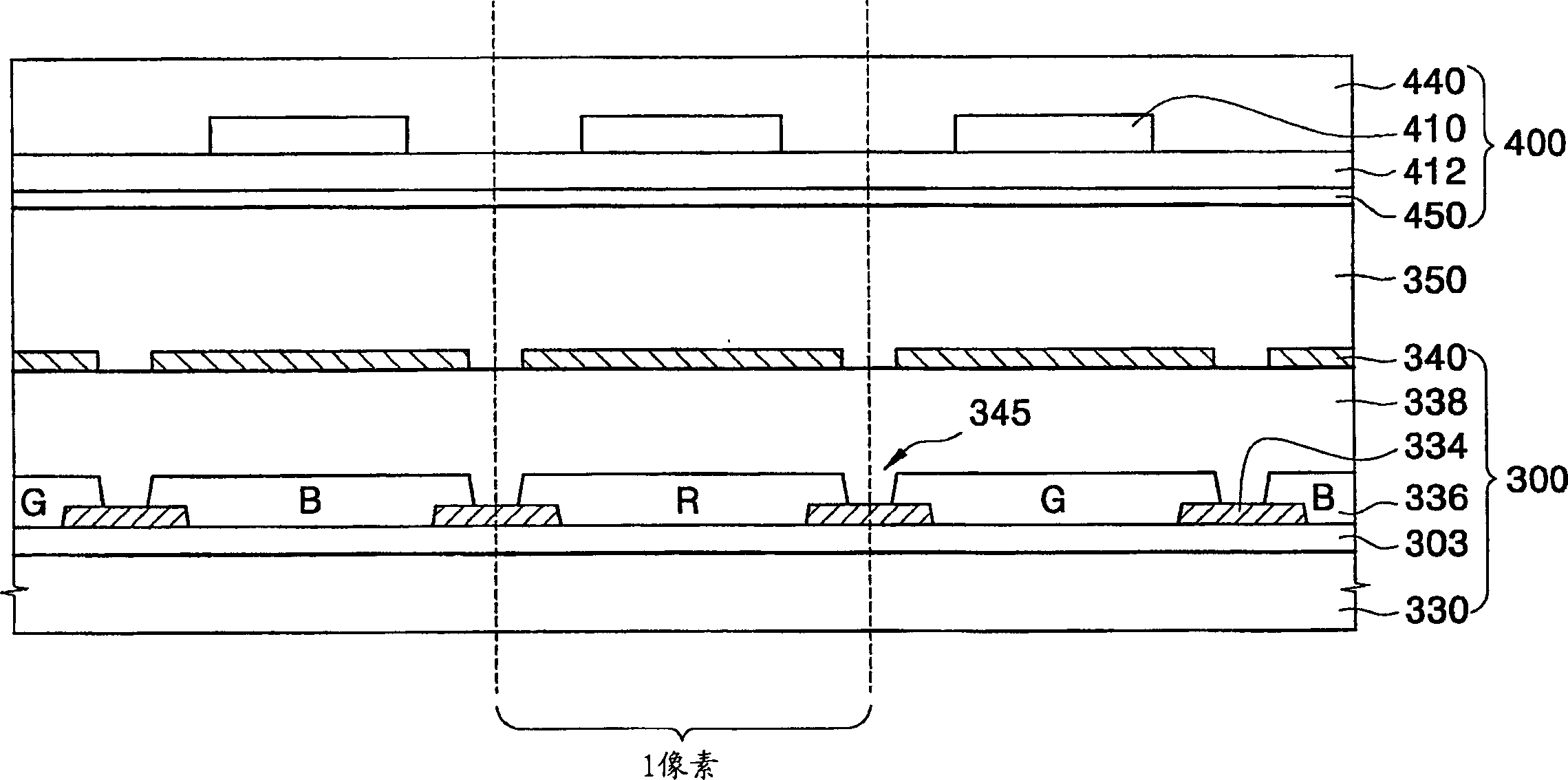
[0045] image 3 is a cross-sectional view showing a color filter structure on an array of an α-Si TFT-LCD panel mounted with a TFT fingerprint recognition substrate according to an exemplary embodiment of the present invention.

[0046] The color filter-on-array structure refers to a structure in which color filters are formed on a TFT substrate so as to be aligned with thin film transistors of the TFT substrate. That is, the color filter and the thin film transistor have a self-aligned structure. Therefore, the aperture ratio of the TFT-LCD panel is increased. In addition, the color filters can be precisely aligned with the thin film transistors of the TFT substrate.

[0047] refer to image 3 , the TFT fingerprint recognition substrate 400 is attached to a TFT-LCD panel having a color filter on array structure.

[0048] The TFT fing...


PUM


Abstract

A liquid crystal display device having fingerprint identification device for enhancing aperture ratio and transmissivity of a TFT-LCD panel is disclosed. A fingerprint identification substrate (400) is attached to a TFT substrate (300). The TFT substrate has color-filter-on-array structure in which the color filters (336) and the thin film transistors can be eliminated, the aperture ratio is increased, and the quality of image display is enhanced. In addition, the transmissivity is increased according to the decrease of the number of glass substrate used in the liquid crystal display device, so that the sensitivity of fingerprint identification is enhanced.

Description

technical field [0001] The present disclosure relates to a liquid crystal display device having a built-in fingerprint recognition device and a method of manufacturing the liquid crystal display device. Background technique [0002] Amorphous silicon (α-Si) thin film transistor liquid crystal display (TFT-LCD) is a type of flat panel display (FPD). α-Si TFT-LCD devices are used in laptops, monitors, televisions and mobile phones. [0003] The α-Si TFT-LCD device displays images by switching thin film transistors. In addition, the α-SiTFT-LCD device also has photosensitive properties and is used as an optical sensor in the field of biometrics. [0004] In the personal authentication system, fingerprint identification using a fingerprint identification device is widely used especially because the fingerprint identification can be implemented at a low cost and is characterized by high usability and high accuracy. [0005] Conventional fingerprint recognition devices can be c...

Claims


Application Information

Patent Timeline
Patent Type & Authority Applications(China)
IPC IPC(8): G02F1/13A61B5/117A61B5/1172G02F1/133G06K9/00
CPCG06K9/0004G02F2001/13312G02F1/13338G02F1/13312G06V40/1318G02F1/13
Inventor 宋溱镐梁成勋蔡钟哲崔埈厚
Owner SAMSUNG ELECTRONICS CO LTD
Learn More