Semiconductor device and method for testing the same

An inspection method and semiconductor technology, applied in semiconductor devices, semiconductor/solid-state device manufacturing, measuring devices, etc., can solve problems such as increased circuit area and LSI mold size

Inactive Publication Date: 2005-11-02
FUJITSU LTD
View PDF3 Cites 3 Cited by
  • Summary
  • Abstract
  • Description
  • Claims
  • Application Information

AI Technical Summary

Problems solved by technology

Therefore, there is a problem that the circuit area increases and the die size of the LSI increases.

Method used


Image

  • Semiconductor device and method for testing the same
  • Semiconductor device and method for testing the same
  • Semiconductor device and method for testing the same

Examples


Embodiment Construction

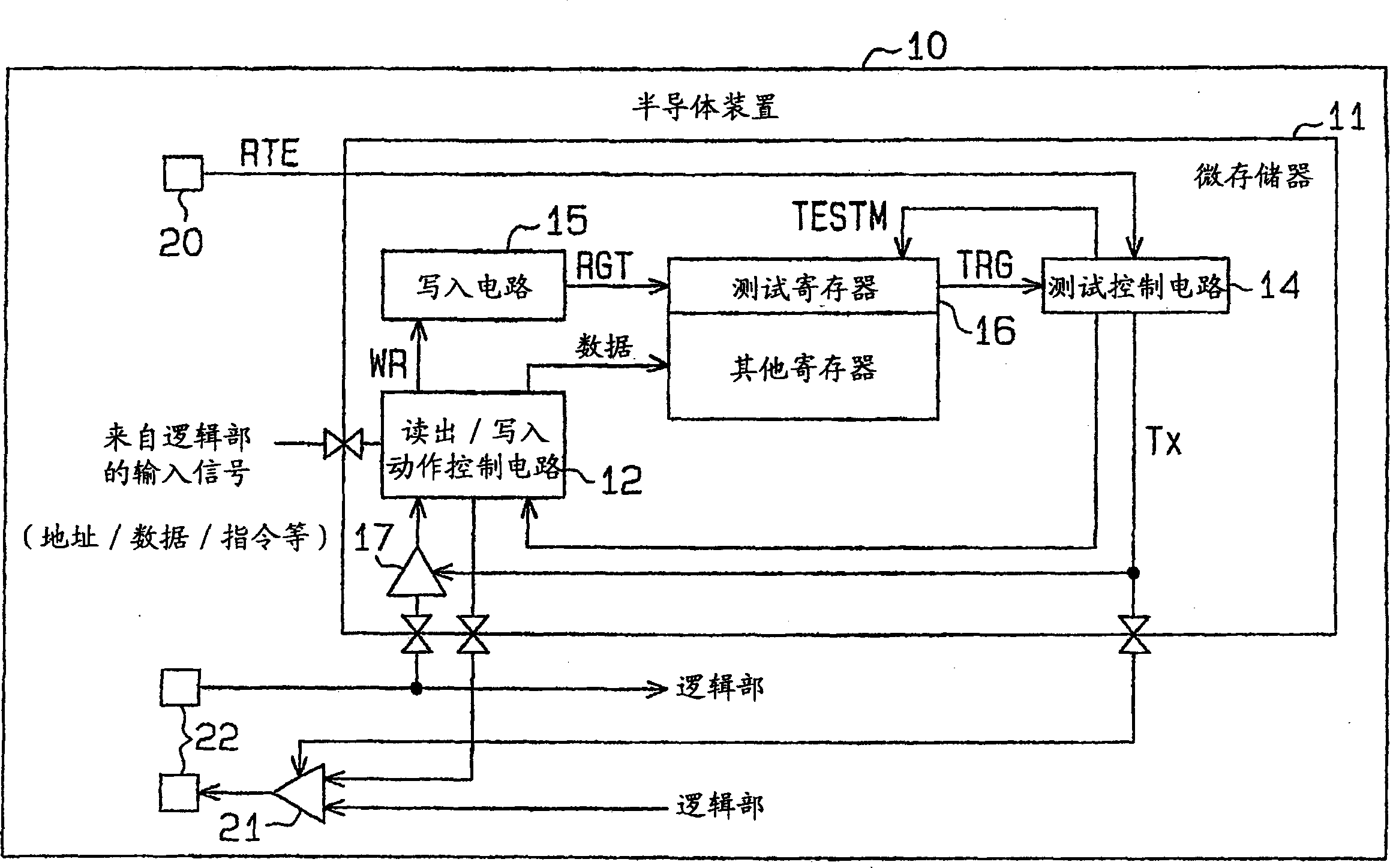
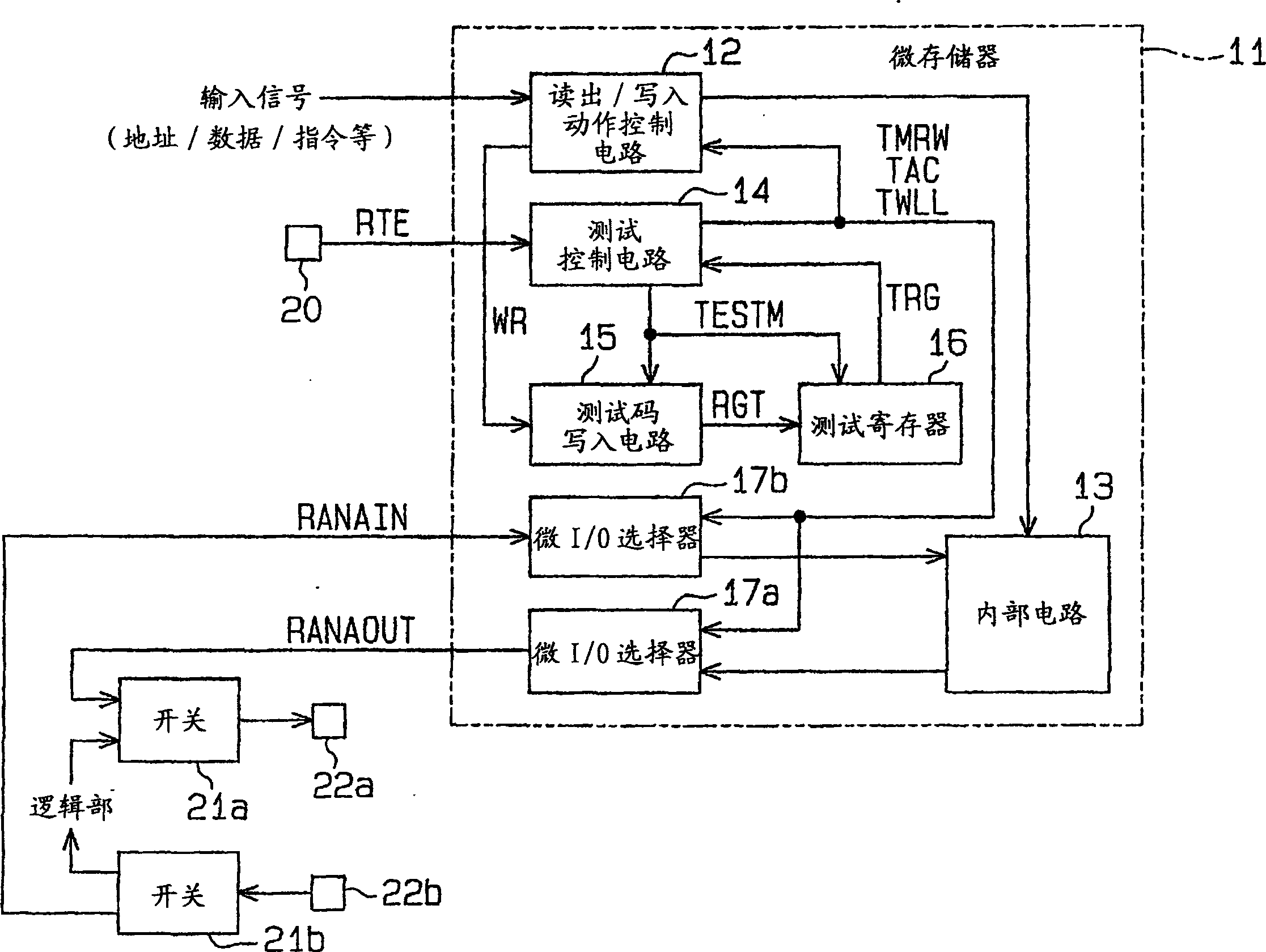
[0030] figure 1 It is a schematic block diagram of a semiconductor device 10 according to an embodiment of the present invention. The semiconductor device 10 has a storage unit (micro memory) 11 mixed with a logic unit. An operation control circuit 12 is provided in the micro memory 11, and the operation control circuit 12 executes data read / write operations based on input signals including addresses, data, and commands. In a storage area (address space) selected by an address contained in an input signal, a test storage circuit 16 is provided, and the test storage circuit 16 stores data for selecting a test mode. The write circuit 15 supplies a control signal RGT allowing data to be written into the test memory circuit 16 in response to a write command WR supplied from the operation control circuit 12 . In the test memory circuit 16, the data Data included in the input signal is written in accordance with the control signal RGT.

[0031] The operation control circuit 12 is...


PUM


Abstract

A semiconductor device wherein a simple circuit arrangement is used to shorten the test time and suppress increase of circuit area required for the test. The semiconductor device (10) has a micro-memory (11) consolidated with a logic part. The micro-memory (11) includes an operation control circuit (12) for executing data read/write operations in accordance with input signals including addresses, data and commands. A storage area of the micro-memory (11) that is selected by an address includes a test register (16) for storing data used for selecting a test mode. A write circuit (15) produces, in response to a write command supplied from the operation control circuit (12), a control signal (RGT) for permitting an operation of writing data into the test register (16).

Description

technical field [0001] The present invention relates to a semiconductor device in which a logic unit and a memory unit are mixed and an inspection method thereof. Background technique [0002] Patent Document 1 JP-A-10-65104 (FIG. 12) [0003] Patent Document 2 JP-A-11-250700 [0004] Patent Document 3 JP-A-2000-57120 [0005] In recent years, semiconductor devices (LSI), such as ASICs and microprocessors, have become highly integrated, and micro memories (storage units) and logic units have begun to be mixed together. Memory mixed LSIs are subject to operational inspection before shipment. This operational inspection tests whether the logic part and micromemory are operating normally. A technique that shortens the inspection time of micromemory with a simple circuit structure is required. [0006] In the mixed memory LSI, normal operations (write operation and read operation) in the micro memory are controlled by signals from the logic unit. For example, when a read com...

Claims


Application Information

Patent Timeline
Patent Type & Authority Applications(China)
IPC IPC(8): G01R31/28G01R31/317G01R31/319H01L21/822H01L27/04
CPCG01R31/31919G01R31/31704G01R31/28
Inventor 古山孝昭
Owner FUJITSU LTD
Why Eureka
Try Eureka